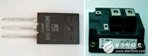
Insulated-gate Bipolar Transistor (IGBT or IGT)
GTR and MOSFET are combined to combine the advantages of both and have good characteristics. Since the advent of the mid-1980s, it has gradually replaced the GTR and a part of the MOSFET market, the leading device for small and medium power power electronic devices.

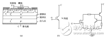
The IGBT is equivalent to a thick base region GTR driven by a MOSFET. From the figure we can also see that there is a parasitic thyristor between the collector and the emitter, and the parasitic thyristor has a holding action. The use of the hole bypass structure and the miniaturization of the width of the emitter region can substantially overcome the holding action of the parasitic thyristor. The low-doped N-drift region of the IGBT is wide, so it can block very high reverse voltages.

IGBT structure, symbol and equivalent circuit
Various protection design methods for IGBTIGBT (Insulated Gate Bipolar Transistor) is a new type of power electronic device that uses MOS to control transistors. It has the characteristics of high voltage, large current, high frequency, small on-resistance, etc., so it is widely used in inverter inverter circuits. in. However, due to the over-current resistance and over-voltage resistance of the IGBT, it can be damaged in the event of an accident. Therefore, it is necessary to protect the IGBT. This paper summarizes the problems related to overcurrent, overvoltage and overheat protection and various protection methods from practical applications. It has strong practicability and good application effect.
1. Overcurrent protection
The manufacturer has strict restrictions on the safe working area provided by the IGBT, and the IGBT is subjected to overcurrent for only a few microseconds (SCR, GTR and other devices are subjected to overcurrent time of several tens of microseconds), and the overcurrent resistance is small. The primary concern with IGBTs is overcurrent protection. The causes of overcurrent are: transistor or diode damage, control and drive circuit failure or interference caused by misoperation, output line connection fault or insulation damage, short circuit, output short circuit to ground and motor insulation damage, inverter bridge Short-circuit of the bridge arm, etc.
There are two cases of overcurrent detection protection for IGBTs:
(1) There is no protection function in the drive circuit. At this time, an overcurrent detecting device is set in the main circuit. For small-capacity inverters, the resistor R is usually directly connected in the main circuit, such as the voltage across the resistor to reflect the current; for large and medium-capacity inverters, due to the large current, the current transformer TA is required. Hall sensor, etc.). The position where the current transformer is connected: one is connected in series in the main circuit like a string resistor; the other is connected in series on each IGBT. The former uses only one current transformer to detect the total current flowing through the IGBT, which is economical and simple, but the detection accuracy is poor; the latter directly reflects the current of each IGBT, and the measurement accuracy is high, but six current transformers are required. The current signal detected by the overcurrent outputs a blocking signal to the control circuit via the optocoupler, thereby turning off the trigger of the IGBT and implementing overcurrent protection.
(2) A protection function is provided in the drive circuit. For example, HR065 of Japan Indah Co., Ltd. EXB840~844 of Fuji Electric, M57962L of Mitsubishi Corporation, etc., is an integrated circuit (called hybrid drive module) that integrates driving and protection functions, and its current detection is utilized in a certain positive direction. Under the gate voltage Uge, the forward voltage drop Uce(ON) is proportional to the collector current Ie, and the size of the Ie is determined by detecting the size of the Uce (ON), and the reliability of the product is high. Different types of hybrid drive modules have different output capabilities, switching speeds and du/dt tolerances. They should be used according to actual conditions.
Since the overcurrent protection threshold voltage action value of the hybrid drive module itself is fixed (generally 7 to 10 V), there is a problem of cooperation with the IGBT. The commonly used method is to adjust the number of diodes V connected in series between the IGBT collector and the driving module, so that the sum of the on-state voltage drops of these diodes is equal to or slightly larger than the overcurrent protection operating voltage of the driving module and the on-state saturation of the IGBT. The difference between the pressure drop Uce (ON).
The above method of adjusting the overcurrent protection operating point by changing the number of diodes is simple and practical, but the accuracy is not high. This is because the on-state voltage drop of each diode is a fixed value, so that the voltage between the driving module and the IGBT collector c cannot be continuously adjusted. In practice, there are two ways to improve:
(1) Change the type of diode to be combined with the number. For example, if the on-state saturation voltage drop of the IGBT is 2.65V and the critical operating voltage of the over-current protection of the driver module is 7.84V, then the sum of the on-state voltage drops across the diode should be 7.84 - 2.65 = 5.19V. Seven silicon diodes are connected in series with one xenon diode. The sum of the on-state voltage drops is 0.7 & TImes; 7 + 0.3 & TImes; 1 = 5.20 V (the silicon tube is regarded as 0.7 V, and the xenon tube is regarded as 0.3 V). Good to achieve cooperation (2) diode and resistor combination. Due to the difference in the on-state voltage drop of the diode, the above improved method is difficult to accurately set the critical operating voltage value of the IGBT overcurrent protection. If one or two diodes are replaced by a resistor, an accurate fit can be achieved.
In addition, because the control signals of the two IGBTs on the same bridge arm overlap or the delay time of the switching device itself is too long, the upper and lower IGBTs are directly connected, and the bridge arm is short-circuited. At this time, the current rising rate and the surge current are very high. Large, extremely damaging IGBTs For this purpose, bridge arm interlock protection can also be set. In the figure, the driving signals of the two IGBTs on the same bridge arm are interlocked with two gates, so that the working state of each IGBT is mutually dependent on the other IGBT driving signal, and only one IGBT is confirmed. After the turn-off, the other IGBT can be turned on, which strictly prevents the occurrence of overcurrent caused by the short of the arm bridge.
2, overvoltage protection
When the IGBT is turned off by the on state, the current Ic suddenly becomes small. Due to the stray inductance in the circuit and the load inductance, a high surge spike voltage uce=L dic is generated at both ends c and e of the IGBT. /dt, plus the IGBT's over-voltage resistance is poor, which will cause the IGBT to break down. Therefore, its over-voltage protection is also very important. Overvoltage protection can be done from the following aspects:
(1) Minimize stray inductance in the circuit. As a module design and manufacturer, it is necessary to optimize the internal structure of the module (such as using a layered circuit, reducing the effective loop area, etc.) to reduce parasitic inductance; as a user, optimize the main circuit structure (using layered wiring, minimize Connection lines, etc.) to reduce stray inductance. In addition, add some low-resistance and low-sensing decoupling capacitors on the entire line to further reduce the line inductance. All of these have a good effect on directly reducing the turn-off overvoltage of the IGBT.
(2) Adopt an absorption loop. The function of the absorption loop is to absorb the energy released in the inductor when the IGBT is turned off to reduce the turn-off overvoltage. There are two commonly used absorption circuits, as shown in Figure 4. (a) is a charge-discharge absorption circuit, and (b) is a clamp-type absorption circuit. For the selection of components in the circuit, in practical work, the capacitor c is selected from high-frequency low-inductance coiled polyethylene or polypropylene capacitors, and ceramic capacitors are also available, and the capacity is about 2 F. The capacitance is chosen to be larger, and the suppression of the surge spike voltage is better, but the assembly time is limited by the discharge time. Resistor R uses oxide film non-inductive resistor, its resistance value is determined to meet the discharge time is significantly less than the main circuit switching cycle requirements, can be calculated according to R ≤ T / 6C, T is the switching cycle of the main circuit. Diode V should use a soft characteristic snubber diode with a low forward transition voltage and a short reverse recovery time.
(3) Appropriately increase the gate resistance Rg. Practice has proved that Rg increases, the switching speed of the IGBT is slowed down, and the switching overvoltage spike can be significantly reduced, but the switching loss is increased correspondingly, so that the IGBT heat is increased, and the overheat protection should be matched. The selection principle of Rg resistance is: when the switching loss is not too large, use a larger resistor as much as possible, and select Rg=3000/Ic in actual work.
In addition to the above-mentioned reduction of the overvoltage between c and e, in order to prevent the gate charge from accumulating and the gate source voltage peaking and damaging the IGBT, some protection components may be disposed between g and e, as shown in FIG. 5. The function of the resistor R is to make the gate accumulate charge discharge, and its resistance value can be 4.7kΩ; two reverse voltage series regulator diodes V1, V2. It is to prevent the gate-source voltage spike from damaging the IGBT.
3, overheat protection
The loss power of IGBT mainly includes switching loss and conduction loss. The former increases with the increase of switching frequency and accounts for the main part of the whole loss; the latter is the product of the average current controlled by IGBT and the power supply voltage. Since the IGBT is a high-power semiconductor device, the power loss causes it to generate more heat (especially when the Rg is selected too large), and the junction temperature of the IGBT cannot exceed 125 °C, and it is not suitable to operate at a higher temperature for a long time, so proper heat dissipation is required. Measures for overheat protection.
The heat dissipation is generally based on a heat sink (including a common heat sink and a heat pipe radiator) and can be forced air-cooled. The structural design of the heat sink should satisfy: Tj=Pâ–³(Rjc+Rcs+Rsa) "Tjm type working junction temperature of Tj-IGBT
Pâ–³-loss power
Rjc-junction-shell thermal resistance vkZ electronic data network
Rcs-shell-heat sink thermal resistance
Rsa-heat sink - ambient thermal resistance
The highest junction temperature of Tjm-IGBT
In practice, we use a combination of a common radiator and forced air cooling, and install a temperature switch on the radiator. When the temperature reaches 75 °C ~ 80 °C, the PMW transmission control signal is stopped by the OFF signal of the SG3525, so that the driver blocks the switching output of the IGBT and turns off the protection.
Hp Probook 450 455 G6 G7,Hp Probook 450 G7 Keyboard,450 G6 Lcd Back Cover,450 G7 Lcd Back Cover
S-yuan Electronic Technology Limited , https://www.syuanelectronic.com