As everyone knows, the performance level of green LEDs does not reach the same red and blue LED. However, black spots can be reduced by reducing current density, using a larger chip, and optimizing growth conditions, and can minimize the distance between LEDs of 190 lm/W at 100 mA drive current. Osram's AndreasL? Ffler and Michael Binder said.
The biggest flaw in LED bulbs is second only to the price that is not ideal. This shortcoming is produced by the process of making white LEDs: the GaN-based blue chip excites the yellow phosphor, mixing the two colors to produce white light. In this way, the red region of the visible spectrum does not contribute much to the light output.
A more advanced method of making white LED lighting products - also a method of solid-state projection display - that is, LEDs made of red, green, and blue, mixed to produce white light. The advantage of this method is that it is not limited to a higher color rendering index, but also achieves higher light efficiency and flexible control of color.
To produce an energy-efficient system in a mixed color, a high-efficiency light source must be used. The performance of blue and red LEDs has been significant, and recent technological improvements have led to peak power conversion efficiencies exceeding 81% and 70%, but the performance of green LEDs is far behind. The phenomenon that such GaN-based LEDs are not highly effective is called a "green light gap."
Green wavelength band
Increasing the efficiency of green LEDs is a major challenge because of the inability to take advantage of the ideal maturity of materials systems. The III-N series used to create high-efficiency blue LEDs will be less efficient at longer wavelengths, while the more efficient Group III phosphides in the red range will face the same distress; The light emitted by the LED emits shorter wavelengths and the efficiency is reduced. In short, the material system is inefficient in the yellow-green spectrum.
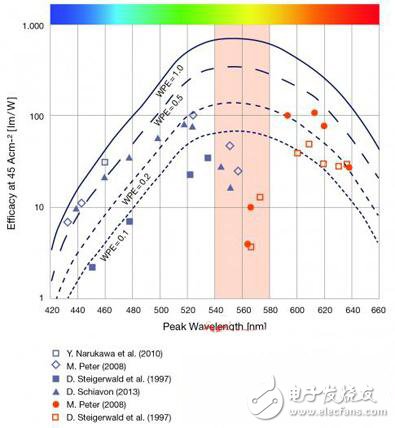
Figure 1: Luminous efficiency of Group III nitrides (green data points) and Group III phosphide LEDs (red light data points) at different wavelengths. The blue line represents the corresponding value of the photometric function of the International Commission on Illumination (CIE) in 1924 multiplied by the electro-optical conversion efficiency (WPE). The yellow-green range is marked with a yellow color and is neither sufficiently covered by the Group II nitride nor by the Group III phosphide. This is the essence of the green gap problem.
For Group III phosphides, emitting light to the green band becomes a fundamental barrier to the material system. Changing the composition of AlInGaP makes it glow green instead of red, orange or yellow—causing insufficient carrier confinement due to the relatively low energy gap of the material system, eliminating effective radiative recombination.
In contrast, Group III nitrides are more difficult to achieve, but the difficulty is not insurmountable. With this system, two factors that cause the efficiency to decrease due to the extension of light into the green band are: external quantum efficiency and electrical efficiency degradation.
The decrease in external quantum efficiency is due to the high forward voltage required for green LEDs. These devices have a very high internal voltage field. Therefore, at a given voltage, the voltage applied to such LEDs will be higher despite the lower bandgap. A higher drive voltage causes the power conversion rate to drop. The second disadvantage is that the green LED decreases as the injection current density increases, which is trapped by the droop effect. The Droop effect also appears in blue LEDs, but the effect is even greater in green LEDs, resulting in lower operating currents.
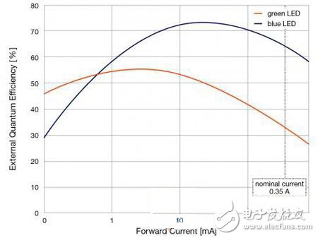
(Fig. 2) Comparison of external quantum efficiency between 1mm2 blue InGaN and green GaN at wavelengths of 442nm and 530nm
The cause of the droop effect has caused intense discussion in the nitride industry. Because the loss rate of the droop effect is cubic dependent on the charge carrier density under electroluminescence and photoluminescence stimulation, most of the guesses point to the Auger recombination as the cause of the droop effect.
However, there are many speculations about the causes of the droop effect, not just the Auger compound, which includes misplacement, carrier overflow or electron leakage. The latter is enhanced by a high voltage internal electric field.
The Single Most Important Thing You Need To Know About Single Sided PCB
As a single sided PCB manufacturer, Jinghongyi PCB has been single sided PCB for many years. Production and manufacturing experience, with a very exquisite single sided PCB Manufacturing process flow chart.
We can produce single-sided copper PCB, single sided copper clad PCB Board , single sided Flex PCB .
We know that when you choose single sided PCB manufacturer, product quality is one of the first factors you need to consider. We are not only engaged in PCB manufacturing for many years, but also one of the large-scale PCB manufacturers in China. We can not only produce single sided PCB, but also double-sided PCB, Multilayer PCB , Aluminum PCB and so on.
In addition to product quality, you may also need to consider the single sided PCB price factor. If you choose us as your partner, you can rest assured that we will be able to provide you with not the best price on the premise of guaranteeing product quality, but the price that we both feel is very reasonable. What do you think?
In this article, we will elaborate on the definition, type, cost components, structure, advantages and disadvantages, manufacturing process and raw materials of single sided PCB. Finally, we will introduce the application of single sided PCB and the differences between single sided PCB and Double Sided PCB . And how to choose between single sided PCB and double sided PCB.
What Is Single Sided PCB
Single-sided PCB diagram mainly used Network Printing(Screen Printing), that is, resist on copper surface, After etching, mark the welding resistance, and then finish the hole and the shape of the part by punching.
Fundamentally, single-sided and double-sided Printed Circuit Boards serve the same purpose. Both serve as catalysts for electrical connections between components, however there are some key differences that set them apart from each other. More specifically, they differ in the costs associated with production and development processes, as well as ampacity differences.
With the appearance of electronic transistor, single sided PCB was developed in the early of 1950, which is mainly manufactured in USA. Single-sided PCB was manufactured by copper etching directly at that time. During 1953 to 1955, Japan use imported copper make out paper phenolic aldehyde copper substrate, and apply mainly on radio products. In 1956, single-sided PCB technology was made big progress with the appearance of professional PCB manufacturers from Japan. In the early stage, copper substrate mainly used paper phenolic aldehyde, but because paper phenolic aldehyde with the factors of low electric insulation, bad solder thermal stability, twist issue etc, paper epoxide resin and glass fiber epoxy resin was developed soon after. Currently, paper epoxide resin is widely used in consuming electronic.
Basically, there is no challenge for PCB manufacturer to produce single sided PCB and the technology is quite mature nowadays. The main focus for PCB manufacturer is how to control production cost and save more cost for customers.
Types of Single Layer PCB
- Single Layer Rigid PCB
It is the type of a single layer PCB which is made up a rigid material such as fiber glass. These PCBs are inflexible and prevent the circuit from bending and breaking. Currently these are used in different types of devices such as in calculators and power supplies etc.
- Single Layer Flexible PCB
It is the type of a single layer PCB which is mode out a flexible material instead of a rigid material and for this purpose plastic materials are used. It has so many advantages over single layer rigid pub but it fabrication cost is so much high.
- Single Layer Rigid Flex PCB
It is the type of a single layer PCBs which is used for high frequency circuits normally in giga hertz. These PCBs are made out a Teflon or polyphenylene oxide (PPO) material. During choosing high frequency single layer PCB many aspects are keep in mind such as dielectric loss, thermal expansion and water absorption etc.
- Single Layer High Frequency PCB
It the type of single layer PCBs which is made out by the combination of plastic and fiber glass. Both materials are combined together into single layer. It has so many advantages over single layer rigid and flexible PCB such as it reduces the weight and size of overall PCB.
- Single Layer Aluminum PCB
What Goes Into Determining single sided PCB Costs and price
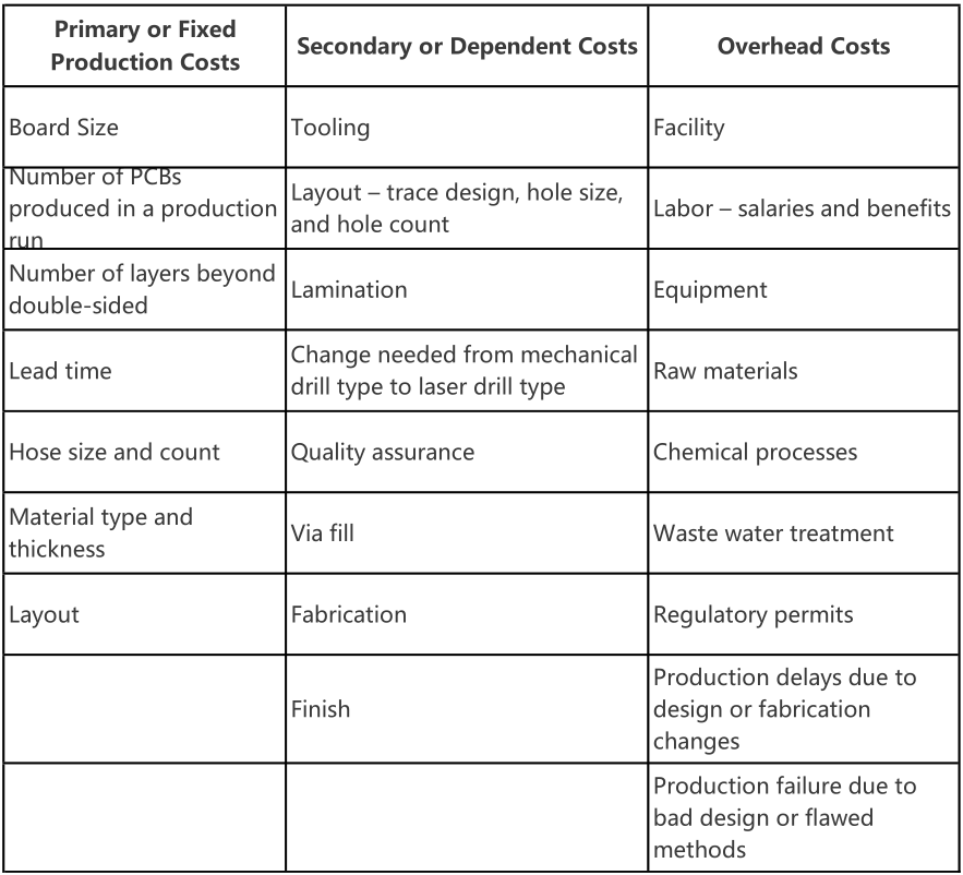
No matter whether manufacturing a single-sided PCB, double-sided PCB, or multilayer PCB, three main cost categories exist: Primary production costs, dependent costs, and overhead costs.
Often, single layer PCB are used for simple devices and usually cheaper than multilayer PCB.
Multilayer PCB has one or multiple conductor patterns inside the board, this increases the area available for wiring. multilayer PCB, such as 4 Layer PCB , 6 Layer PCB and 8 Layer PCB are usually used for more complicated devices. For example, smart phones use 12 layers due to the various demands of the circuit. As a result, multilayer PCB circuit boards are more expensive.
You can break them down into the following categories:
Layout alters the cost balance. While the number and size of holes remain the same with single-sided PCBs, two different circuit designs on one substrate change the number of holes and add vias.
Because double-sided PCBs welcome complex circuit designs, layout also becomes a dependent factor. As the number of traces increase, costs increase. Smaller surface mount components fastened to the bottom side change the trace spacing. As the space between the traces narrows, costs can jump 5 to 10 percent.
Different layouts may require different hole sizes and the use of laser rather than mechanical drills. Smaller hole sizes and larger hole counts drive the cost higher because of a change in the manufacturing process.
Advantages of Single Sided PCB
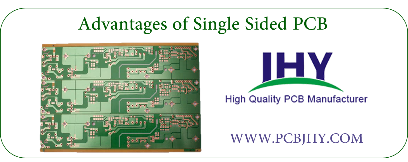
- Simple and easy to design and install
- Lower cost, especially for high volume orders
- Easy drilling, soldering, de-soldering and components inserting process
- Lower probability of manufacturing issues,such as short circuiting and producing noise
- Components are installed at only one side, require lower jumper to compensate the circuit
- Popular, common, and easily understood by most PCB manufacturers
- Less time for fault tracing and repairing
Single Layer PCB Disadvantages
Despite their cost advantages and other perks, single-layer boards are not the right choice for every project due to the limitations they have, which include:
- Simplistic Design: The simplicity of single-layer boards' is one of their biggest benefits, but it's also a substantial limitation. For more complex devices that require a higher number of components and connections, a single layer does not provide enough space or power. If wires cross each other, the device won't function properly, so it's critical that the board has enough space to accommodate everything. More complex designs just can't fit on single-sided PCBs.
- Slower Speed and Lower Operating Capacity: The limited number of connections on these boards also affects their power and speed. These less-dense designs are not as robust as those with more circuits and have a lower operating capacity. They might not have enough power for some applications.
- Larger Size and Higher Weight: To add capabilities to a single-sided board, you need to expand its dimensions rather than add another layer, as you could with you a multi-layer PCB. You could use multiple separate boards, but one multi-layer board could likely handle the same requirements. Increasing the size or number of boards in a device also increases your final product's weight.
How to make single sided PCB
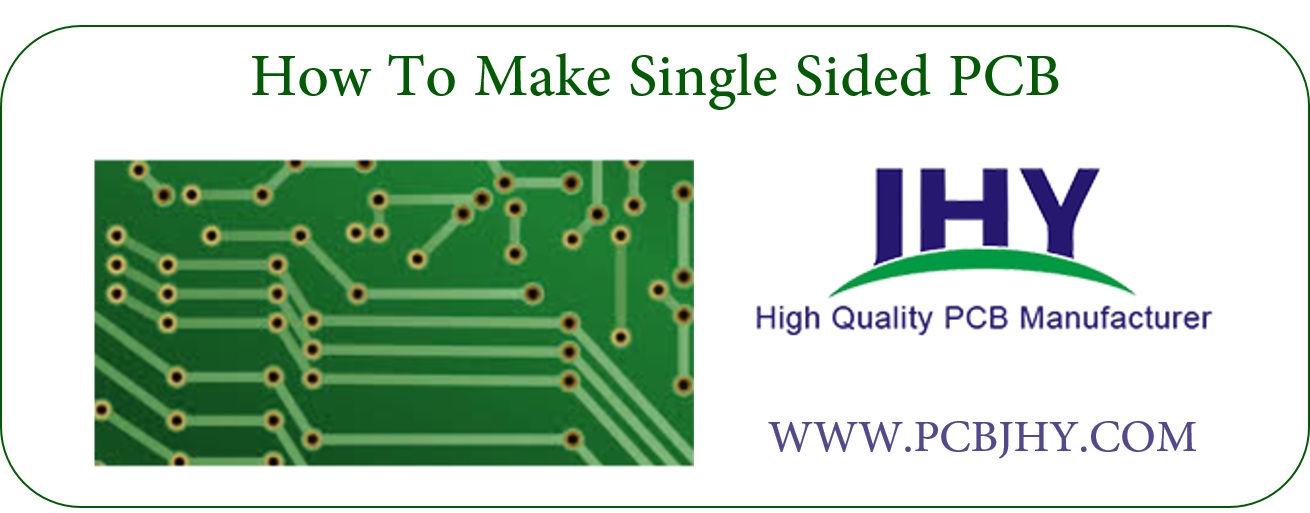
Single sided PCB manufacturing Process flow chart
One thin layer of thermally conductive but electrically insulating dielectric is laminated with copper. Soldermask is usually applied on top of the copper.
Cutting - Cleaning - Drilling - Cleaning - PTH - Panel - Plating - Cleaning - Photolithography - Image Transfer - Inspection - Copper/Tin - Plating - Coating - Removing/Etching/Tin - Removing - Inspection - Cleaning - Solder - Mask - Exposure/Develop/Inspection - Prepreg - Screen - HASL - Conformal - Coating - Post - Soldering - Cleaning - Test - Final Inspection - Packing
Single layer PCB Raw Material
- Fr4 Grade Fiberglass Laminates
- Aluminum
- Copper base
- Cem 1
- Cem 3
Construction of Single Sided PCB
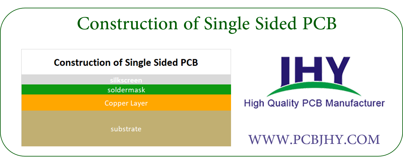
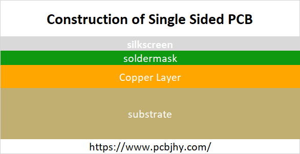
The base material, which is also named as substrate, is composed of insulating fiber glass which gives PCB strength and compact look. The nature and type of base material defines if board is going to be Flexible PCB or Rigid PCB.
Above substrate, there lies a copper layer which provides conducting path for various components on the board. The copper thickness is different for different boards depending on your needs and requirements and is defined in ounces per square foot.
On the top of copper foil, there exists a solder mask layer. This layer is mainly used for protection and makes the copper foil insulating which helps in avoiding the conduction in case direct contact happens with some conducting material.
On the top of all layers, there exists a silkscreen layer that is mainly used for adding symbols and characters on the board so a common person can anticipate the clear understanding of the board.
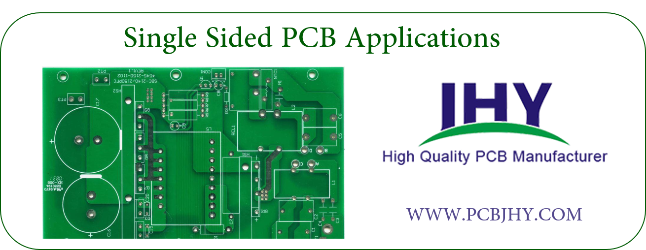
Single-Sided PCB Applications
- Vending machines
- Camera systems
- Surveillance
- Calculators
- Printers
- Solid state drives
- Coffee makers
- LED lighting
- Packaging equipment
- Sensor products
- Power supplies
- Relays
- Radio and stereo equipment
- Timing circuits
What Is Double-Sided PCB
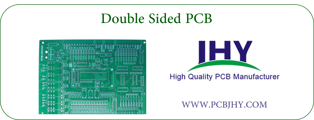
It need circuits on both sides. Via is the holes on boards, coated with metal and it can connect wires on both sides. Because the area of Double-sided PCB is twice as large as the Single-sided PCB, and because the wiring is interleaved, which is better suited for circuits that are more complex.
Someone may feel confused that if one Double-sided PCB, wires on both sides while Electronic parts only one side, is this a Double-sided board or a single onel? The answer is obvious. This kind of board is a Double-sided board, it's just install a component on the Double-sided board.
Differences Between Single sided PCB and Double sided PCB
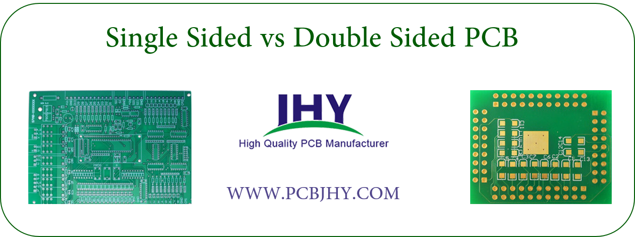
single sided vs double sided PCB
Single and double sided printed circuit boards share the same material make-up: FR-4, which is a form of fiberglass mixed with epoxy. In modern manufacturing, this is usually layered with copper for conductivity and then coated in solder mask for a professional finish. Sometimes, in a process called silk screening, industrial printers print markings and labels on the board as well.
Single-sided PCBs consist of the FR4 insulating core substrate and a thin layer of copper coating on the bottom or solder-side of the substrate. Through-hole components mount on the top or component-side of the substrate with the leads passing through to the bottom side and soldered to the copper pads and tracks. Surface mount components mount directly to the solder side. The primary difference between the two boards will be in conductor placement.
Double-sided boards rely on the same core substrate but have conductors on both sides of the substrate. Very simply, a double-sided board delivers twice the area for conductors. Complex routing can occur with through-hole components mounted on the top layer and surface mount components mounted on the bottom layer. Plated through holes establish [vias" or the electrical connections between the two sides.
Choose Single Sided PCB or Double Sided PCB?
Which PCB you pick depends on your needs and requirements. Sometimes single sided PCBs are more suitable for project design as compared to double sided PCBs and vice versa.
Before you pick any type of PCB for your project, you must take one thing into consideration that single sided PCB layouts are more difficult to route as compared to double sided PCB, but following are the reasons why you should put an effort for making and picking single sided PCB over other PCBs.
- If you are hobbyist or students, and concerned to make PCB at home, you must know, developing single sided PCBs at home are much easier than developing double sided PCBs at home.
- As you are a manufacturer and very much interested to keep your cost down and producing a single sided PCB a most economical process. In terms of cost, producing single sided PCBs are more economical than producing double sided PCBs.
- Almost all HVAC systems make use of single sided PCBs, because they are more reliable and cost effective and don`t compromise the overall quality of the product.
- Using through hole technology in single sided PCBs still have its drawbacks and limitations because conductive layers, lines and pads stay on single side of PCB but it still is a cheap process to combine all components at one place. Multilayer PCB is also used in many applications where single sided and double sided PCBs fail to fulfill the requirements.
Relationship Resources
Multilayer Metal Core PCB
Single Layer Metal Core PCB
Single Sided Flexible PCB
Single Sided PCB
Single Sided PCB, Single Layer PCB, 1 Layer PCB, making circuit boards
JingHongYi PCB (HK) Co., Limited , https://www.pcbjhy.com