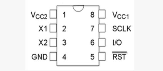
X1 X2 32.768KHz ———— Crystal Pin
GND --- Ground
RST ———— Reset foot
I/O --- Data Input/Output Pins
SCLK --- Serial Clock
Vcc1, Vcc2 ————Power Supply Pins
The DS1302 has pin assignments where Vcc2 is the main power supply and VCC1 is the backup power supply. With the main power off, the continuous operation of the clock can also be maintained. DS1302 is powered by the larger of Vcc1 or Vcc2. When Vcc2 is greater than Vcc1+0.2V, Vcc2 supplies power to the DS1302. When Vcc2 is less than Vcc1, DS1302 is powered by Vcc1.
X1 and X2 are oscillating sources, external 32.768kHz crystal. RST is the reset/chip select line and all data transfers are initiated by setting the RST input drive high. The RST input has two functions: First, the RST turns on the control logic, allowing the address/command sequence to be sent to the shift register; second, the RST provides a method to terminate single-byte or multibyte data transfers.
When RST is high, all data transfers are initiated, allowing the DS1302 to operate. If RST is driven low during the transfer, the data transfer will be terminated and the I/O pin will be in a high-impedance state. During power-up operation, RST must be held low before Vcc 2.0V. RST can only be asserted high when SCLK is low.
I/O is the serial data input/output (bidirectional), and SCLK is the clock input.
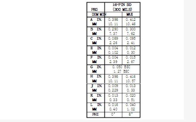
DS1302 Package Information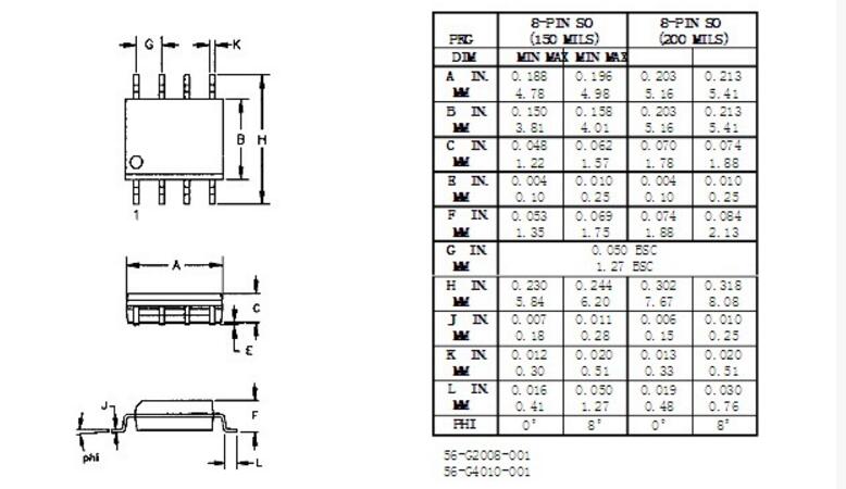
The circuit of the DS1302 is a clock circuit. The crystal used by the DS1302 is a 32.768k crystal. No external capacitor or resistor circuit is added to the crystal. The accuracy of the clock first depends on the crystal's accuracy and the pin's load capacitance. If the crystal oscillator is inaccurate or the load capacitance is too small, the clock error will be too large. After all this has been done, one final consideration is the temperature drift of the crystal. As the temperature changes, the crystal often changes in accuracy. Therefore, in an actual system, one of the methods is often proofread. For example, we use the computer's clock, usually we will set an option "set the computer to internet time synchronization." After selecting this option, it is generally possible for our computer to synchronize with the internet time calibration after a period of time.
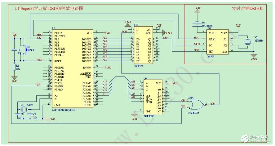
1 pin VCC2 is the positive pin of the main power supply. 2 pin X1 and 3 pin X2 are the crystal input and output pins, 4 pin GND is the negative pin, 5 pin CE is the enable pin, then the IO port of the SCM, 6 pin I /O is the data transfer pin, then the IO port of the MCU, 7-pin SCLK is the communication clock pin, and then the IO port of the MCU. The 8-pin VCC1 is the backup power pin. Considering that the KST-51 development board is a learning-oriented board, and that the backup battery is inconvenient for air transportation and transportation, the 8-pin is not connected to a backup battery, but instead a 10uF capacitor is connected. This capacitor is equivalent. In a battery with a small battery, after testing and testing, it can maintain the DS1302 running for about 1 minute after the system is powered off. If you want to run for a long time, you can increase the capacity of the capacitor or replace it with a backup battery. After the electricity is not needed, it can be kept running, or it can be left floating, as shown in Figure 15-7 and Figure 15-8.
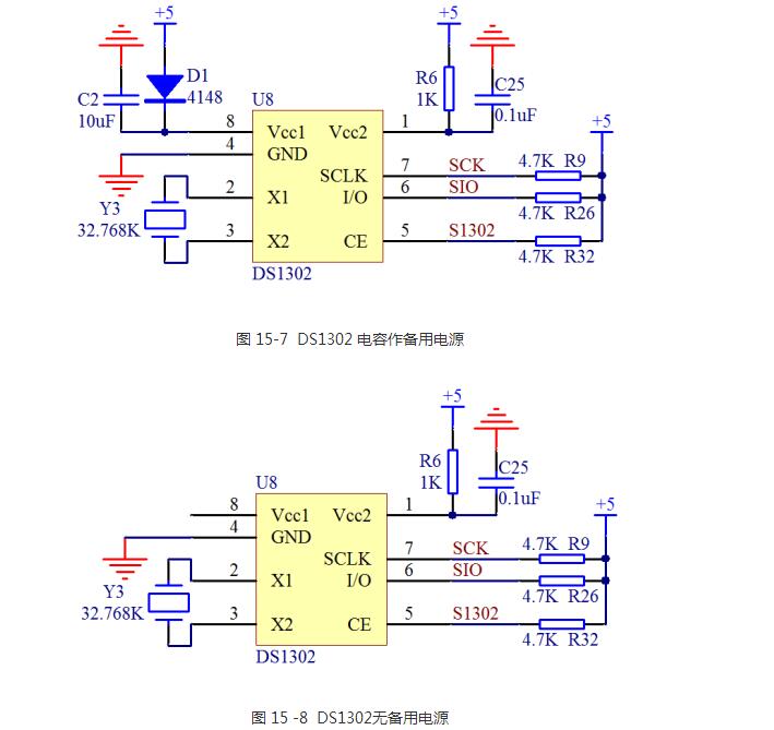
The trickle charge function is basically not used, because in practical applications, rechargeable batteries are seldom used as backup power sources. The cost is too high. This course will not be covered. When we use it, we use a 5V power supply directly to connect a diode. When the main power supply is powered on, the capacitor is charged. In the case of main power failure, the diode can prevent the capacitor from discharging to the main circuit, and it is only used to maintain the power of the DS1302. The greatest use of this circuit is to keep the real-time clock running without interruption in the battery-powered system when replacing the main battery. A 1-minute period is enough for battery replacement. In addition, through our experience, connecting a 1K resistor in series with the main power pin of the DS1302 can effectively prevent the power supply from impacting the DS1302. R6 is this resistor, and R9, R26, and R32 are pull-up resistors.
DS1302 write timingThe year, month, day, minute, and second information is written by command. The command format is 2 bytes. The first byte is the address and the second byte is the content.

Write logic:
1 Pull RST down first
2 Pull SCLK low (if not pulled low, and it was originally high, a bit was sent instantaneously. We haven't put data yet)
3 Then RST pulls up. . Form a rising edge
4 Put a bit (byte transmission order, from low to high) at the IO port
5 Let SCLK be high and form a rising edge. At this time, DS1302 will read the data of IO port into its register.
6 Pull SCLK low to prepare for the next byte. Jump to 5 until all 16 bytes have been sent
7 Pull RST low to complete the entire write process.
DS1302 command format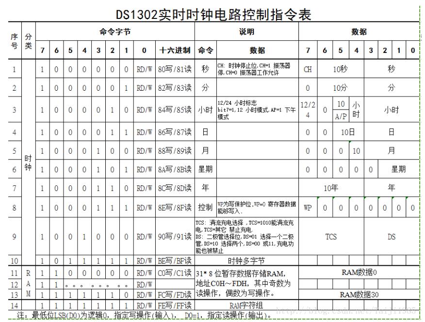
Although the command byte may seem complicated, writing the program is as simple as setting the second to 13 seconds. What should be the two bytes of data that are sent? The first byte is 0x80 (the command to write the second, see above). The second data, the fourth position is 3, and the high position is 1. Is (1<<4)|3, which is 0x13
Other year, month, and day are similar. Let's talk about a few special places.
(1) If you want to stop the watch
Send a command to set the second, the highest position of the second byte is 1, ie, send 0x800x80.
(2) The highest bit of the second byte of the hour controls 12 or 24 hex
Arduino controls DS1302 connection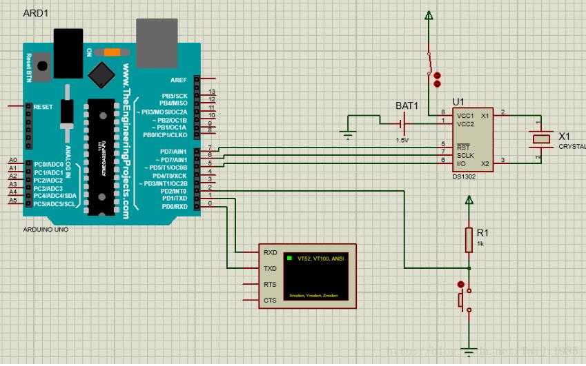
/* * Read and write DS1302 clock chip
* @author Yangtf
* Great document http://DS1302/data/185858.html
* Sequence diagram http://
*
*/
#define RST 7
#define SCLK 6
#define IO 5
//#define L(item) digitalWrite((item),LOW)
//#define H(item) digitalWrite((item),HIGH)
#define uchar unsigned char
Void setup() {
pinMode(RST,OUTPUT);
pinMode(SCLK,OUTPUT);
pinMode(IO,OUTPUT);
Serial.begin(9600);
attachInterrupt(0, settm, FALLING );
}
Void writeData(unsigned char addr, unsigned char dat)
{
pinMode(IO,OUTPUT);
digitalWrite(RST,LOW); //pull down, then pull up
digitalWrite(SCLK,LOW) ; // rising edge of SCLK, the chip will read IO port d
elayMicroseconds(1);
digitalWrite(RST,HIGH);
Int i;
For(i =0;i"8;i++)
{
digitalWrite(SCLK,LOW);
digitalWrite(IO, addr&1);
Addr =addr""1;
digitalWrite(SCLK,HIGH);
delayMicroseconds(1);
}
For(i =0;i"8;i++){
digitalWrite(SCLK,LOW);
digitalWrite(IO, dat&1);
Dat =dat""1;
digitalWrite(SCLK,HIGH);
delayMicroseconds(1);
}
digitalWrite(RST,LOW);
}
Uchar readData(uchar addr){
Addr = addr | 1; // The lowest position for reading is 1
pinMode(IO,OUTPUT);
digitalWrite(RST,LOW); //pull down, then pull up
digitalWrite(SCLK,LOW) ; // rising edge of SCLK, chip will read IO port
delayMicroseconds(1);
digitalWrite(RST,HIGH);
Int i;
For(i =0;i"8;i++){
digitalWrite(SCLK,LOW);
digitalWrite(IO, addr&1);
Addr =addr""1;
digitalWrite(SCLK,HIGH);
delayMicroseconds(1);
}
pinMode(IO,INPUT);
Int dat = 0;
For(i =0;i"8;i++){
digitalWrite(SCLK,LOW);
delayMicroseconds(10);
Uchar b = digitalRead(IO);
Dat = dat "" 1; // pan first
Dat = dat | (b "7"; / / put the income into the highest position
digitalWrite(SCLK,HIGH);
delayMicroseconds(1);
}
digitalWrite(RST,LOW);
Return dat ;
}
#define SECOND 0x80
#define MIN 0x82
#define HOUR 0x84
#define DAY 0x86
#define MONTH 0x88
#define YEAR 0x8C
#define WEEK 0x8A
Void writeTImeUnit(
Uchar TYPE,uchar data){
Uchar high = data / 10;
Uchar low = data % 10;
Uchar d = ((data /10) "4) | (data % 10);
writeData(TYPE,data);
}
Uchar readTImeUnit(uchar TYPE){
Uchar r = readData(TYPE);
r = 10*(r "" 4)+ (r & 0xf);
Return r;
}
Void writeAllTm(uchar tm[]){
Uchar s = SECOND;
For(uchar i=0;i“5;i++){
writeTImeUnit(s,tm[5-i]);
s+=2; } writeTImeUnit(YEAR,tm[0]);
} void readAllTm(uchar tm[]){
Uchar s = SECOND;
For(uchar i=0;i“5;i++){
Tm[5-i] = readTimeUnit(s);
s+=2;
}
Tm[0] = readTimeUnit(YEAR);
Tm[6] = readTimeUnit(WEEK);
}
Void printTm(uchar tm[]){
Serial.print(tm[0]);
Serial.print("-");
Serial.print(tm[1]);
Serial.print("-");
Serial.print(tm[2]);
Serial.print(" ");
Serial.print(tm[3]);
Serial.print(":");
Serial.print(tm[4]);
Serial.print(":");
Serial.print(tm[5]);
Serial.print(" week ");
Serial.print(tm[6]);
Serial.println();
}
Uchar st = 0;
Void loop() {
Uchar tm[7] = {0};
readAllTm(tm);
printTm(tm);
Delay(1000);
}
Void settm()//Interrupt Function
{
Uchar tm[] = {11,12,13,4,5,6 ,0}; // 2011-12-22 3:4:1
Serial.println("set tm ...");
writeAllTm(tm);
}
SHENZHEN CHONDEKUAI TECHNOLOGY CO.LTD , https://www.szsiheyi.com