The current mainstream FPGAs are still based on look-up table technology, which has far exceeded the basic performance of previous versions, and integrates hard-core (ASIC-type) modules of common functions such as RAM, clock management and DSP. The FPGA chip is mainly completed in 7 parts: programmable input and output unit, basic programmable logic unit, complete clock management, embedded block RAM, rich routing resources, embedded underlying functional unit and embedded dedicated hardware module. .
Fpga chip system structure diagram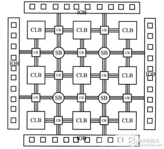
The programmable input/output unit is referred to as the I/O unit, which is the interface part between the chip and the external circuit. It performs the driving and matching requirements of the input/output signals under different electrical characteristics. The schematic structure is shown in the figure below. The I/O within the FPGA is categorized by group, and each group can independently support different I/O standards. Through the flexible configuration of the software, different electrical standards and I/O physical characteristics can be adapted, the driving current can be adjusted, and the upper and lower pull-down resistors can be changed. Currently, the frequency of I/O ports is getting higher and higher, and some high-end FPGAs can support data rates up to 2Gbps through DDR register technology.
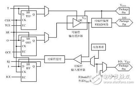
IOB internal structure
The external input signal can be input to the FPGA through the memory unit of the IOB module or directly into the FPGA. When an external input signal is input to the FPGA through the memory location of the IOB module, the hold time (Hold TIme) requirement can be reduced, usually by default to zero. In order to manage and adapt to various electrical standards, the IOB of the FPGA is divided into several banks. The interface standard of each bank is determined by its interface voltage VCCO. A bank can only have one type of VCCO, but VCCOs of different banks can different. Only ports of the same electrical standard can be connected together, and the same VCCO voltage is the basic condition of the interface standard.
2. Basic programmable logic unitThe basic programmable logic unit of the FPGA is composed of a lookup table (LUT) and a register (Register), and the lookup table performs pure combinatorial logic functions. The FPGA internal registers can be configured as either synchronous/asynchronous reset and set, clock-enabled flip-flops, or as latches. FPGAs typically rely on registers to complete synchronous timing logic design. In general, the configuration of the more basic basic programmable unit is a register plus a lookup table, but the internal structure of the registers and lookup tables of different manufacturers are different, and the combination mode of the register and the lookup table are also different.
One important significance of learning the LUT and Register ratios of the underlying hive is device selection and size estimation. In addition to the basic programmable logic unit, there are embedded RAM, PLL or DLL, dedicated Hard IP Core, etc., these modules can also be equivalent to a certain size of the system door, so the simple scientific method is The number of registers or LUTs of the device is measured.
3. Digital Clock Management Module (DCM)Digital clock management is available in most FPGAs in the industry (all of Xilinx's FPGAs have this feature). Xilinx offers state-of-the-art FPGAs that provide digital clock management and phase loop locking. Phase loop locking provides accurate clock synthesis and reduces jitter and filtering.
4. Embedded Block RAM (BRAM)Most FPGAs have embedded block RAM, which greatly expands the range and flexibility of FPGA applications. The block RAM can be configured as a common storage structure such as single port RAM, dual port RAM, content address memory (CAM), and FIFO. The CAM memory has a comparison logic in each of its internal memory cells. The data written to the CAM is compared with each of the internal data and returns the address of all data identical to the port data, thus the address at the route. There are a wide range of applications in the switch. In addition to the block RAM, the LUT in the FPGA can be flexibly configured into a structure such as RAM, ROM, and FIFO. In practical applications, the amount of internal block RAM in the chip is also an important factor in selecting a chip.
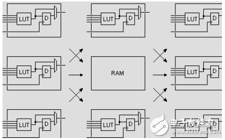
Embedded block RAM
ZGAR PCC KIT
ZGAR electronic cigarette uses high-tech R&D, food grade disposable pod device and high-quality raw material. All package designs are Original IP. Our designer team is from Hong Kong. We have very high requirements for product quality, flavors taste and packaging design. The E-liquid is imported, materials are food grade, and assembly plant is medical-grade dust-free workshops.
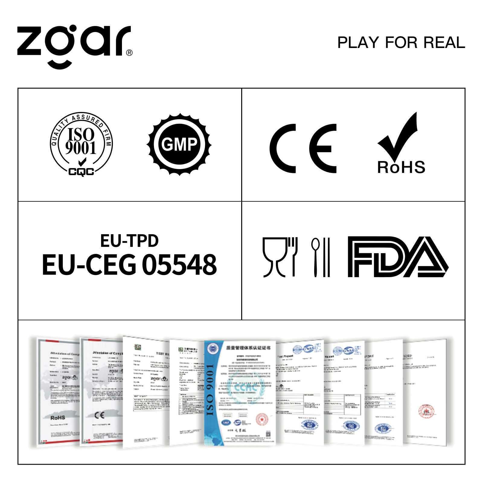
From production to packaging, the whole system of tracking, efficient and orderly process, achieving daily efficient output. We pay attention to the details of each process control. The first class dust-free production workshop has passed the GMP food and drug production standard certification, ensuring quality and safety. We choose the products with a traceability system, which can not only effectively track and trace all kinds of data, but also ensure good product quality.
We offer best price, high quality Vape Device, E-Cigarette Vape Pen, Disposable Device Vape,Vape Pen Atomizer, Electronic cigarette to all over the world.
Much Better Vaping Experience!
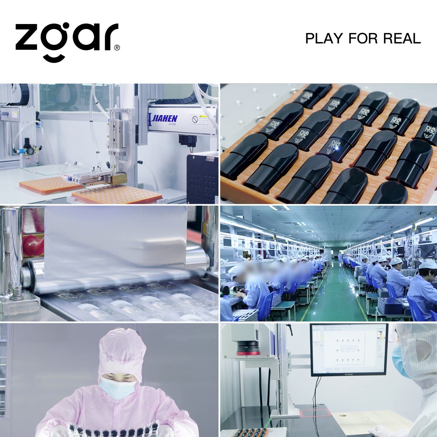
E-Cigarette Vape Pen,Disposable Device Vape,PCC SET, Vape Pen Atomizer,Latest Disposable E-Cigarette OEM vape pen,OEM electronic cigarette
ZGAR INTERNATIONAL(HK)CO., LIMITED , https://www.sze-cigarette.com