In sharp contrast to the “soft†mobile chips represented by smartphones, the market for semiconductor components associated with the IoT-linked subsystems and network communication, sensing and control functions within various devices has grown significantly. Based on the huge market potential of the Internet of Things, mobile phone chip manufacturers have begun to exert their strength. The traditional mobile phone chip manufacturers and the industry are using the Internet of Things as a new growth opportunity. It is precisely because of the active participation of the industry's big players, the ecology of the Internet of Things. The system is maturing.
IoT think tank editor Xiao Xiangxiang yesterday's original article "Intelligent Hardware Industry Alarm: Beware of Mobile Phone Manufacturers Group Attack", from the shrinking process of the mobile phone manufacturers market, led to a number of chip manufacturers 暧昧 mergers and acquisitions love and hate story. Indeed, chip makers that have seen rapid growth in smartphone and tablet shipments in the past have had to think about new growth opportunities in the context of the increasingly saturated mobile phone market. The imagination of tens of billions of smart connected terminals in the future will also bring new blue oceans to chip manufacturers. Let's take a look at the views of the well-known IT expert Sun Yongjie on this phenomenon:
As the global smartphone market slows down, the days of closely related chip makers are beginning to be “softâ€. Following last quarter, major mobile phone chip makers such as Qualcomm and MediaTek all experienced a decline in revenue and profits. Recently, there have been rumors that chip maker Marvell may be sold. In addition, Broadcom, Nvidia and others have successively announced their withdrawal from the mobile phone chip market. While the mobile phone chip industry and related manufacturers are accelerating integration, what is the future or the new blue ocean?

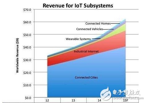
In sharp contrast to the "soft" mobile chips represented by smartphones, according to the latest forecast report from market research firm IC Insights, the subsystems linked to the Internet of Things (IoT) communicate with each other within the network. The market size of semiconductor components related to measurement and control functions is expected to grow by 29% in 2015 to reach US$62.4 billion.
It is based on the huge market potential of the above IoT that mobile phone chip manufacturers have begun to exert their strength. For example, in the last quarter's earnings report, Qualcomm said that it will strengthen management in the future, that is, focus on investing in smart phone chips and related growth opportunities, such as leading modems and other differentiated technologies, focusing on the highest return opportunities. Includes data centers, small cells and some vertical IoT investments. The £1.6 billion acquisition of the British chipmaker CSR (mainly focusing on voice/music, low-power Bluetooth, in-vehicle systems, indoor positioning and document imaging chips) has been the best proof of this strategy.
In fact, Qualcomm has quietly achieved $1 billion in revenue on IoT chip sales last year, and its chips are used in various urban infrastructure projects, home appliances, automobiles and wearables. It is said that a total of 120 million smart home devices equipped with Qualcomm chips were shipped last year. In addition, 20 million cars and 20 wearable devices use Qualcomm chips, and 10% of this year's chip business revenue will come from IoT devices other than smartphones.
In addition to Qualcomm, Samsung also announced the system-level chip ArTIk for IoT devices. It is worth mentioning that behind this chip is the software ecosystem that it is building, the SmartThings IoT cloud and development kit acquired by Samsung (developers can apply here now), and a large number of partners: Arduino and Arduino IDE, Tembook software stack, Internet One analysis platform Medium One, SigFox for wireless connection to the Internet of Things.
Referring to the ecosystem, Microsoft has taken the lead in the IoT operating system, which will launch an operating system called Windows 10 IoT Core (IoT Core Edition) that runs on ATMs, ultrasound devices and wearable devices. In contrast, Google launched a new Internet of Things program at this year's Google I/O conference, which was named Project IoT (Internet of Things). At the HNC2015 network conference held recently, Huawei demonstrated the Agile IoT system, including an operating system called LiteOS that controls basic equipment. This is Huawei's most important step toward the Internet of Things. The Internet of Things has attracted heavyweight companies such as Google, Intel and IBM to join their respective standards and communication protocols.
It is not difficult to see from the above that not only the traditional mobile phone chip manufacturers, but the industry is using IoT as a new growth opportunity, and it is because of the active participation of the industry's big players that the IoT ecosystem is maturing.
In addition to IoT, the recent acquisition of Altera by the chip giant Intel's $16.7 billion indirectly proves the potential of another huge chip market, namely the server chip-based data center and cloud computing market.
As we all know, the decline of the traditional PC market has caused Intel's revenue and profits in this chip market to decline. At the same time, the mobile chip market represented by smart phones is also unfavorable. Despite this, Intel has benefited from the growth in the server chip market (the increase in mobile devices is changing the application model while promoting the demand for server chip-based data centers and cloud computing markets), and its overall performance is still cited. People pay attention. Based on this, IBM, which has sold its chip manufacturing facility, has opened up its own Power chip in order to gain a share of this market with the help of partners. Similarly, mobile phone chip makers have also turned their attention to this market. Previously, Samsung, NVIDIA and other companies tried to enter this market, but ultimately lost due to many factors such as technology and market. As a result, the industry's most challenging and threatening expectations for Intel in this market are pinned on Qualcomm.
In fact, as early as last year, Qualcomm claimed to enter the server chip market to compensate for the loss caused by the slowdown in the growth of the mobile phone chip market. With the recent conclusion of a memorandum of understanding with Guizhou Province of China, the establishment of an independent Chinese legal entity, the development and sale of a chipset based on Qualcomm's ARM-based server technology for use in China, It indicates that Qualcomm will formally cooperate with relevant partners in China in the server chip market. Of course, in addition to Qualcomm, MediaTek, its biggest competitor in the mobile phone chip market, is also reportedly planning to enter the server chip market.
In summary, we believe that when the growth rate of the mobile phone market slows down, the diversification of traditional mobile phone chip manufacturers will be the inevitable choice for their future survival and development, and the IoT and data center markets will undoubtedly be the most important blue ocean, who With the early deployment and exertion in the above-mentioned fields, it is possible for anyone to be invincible in the future competition.
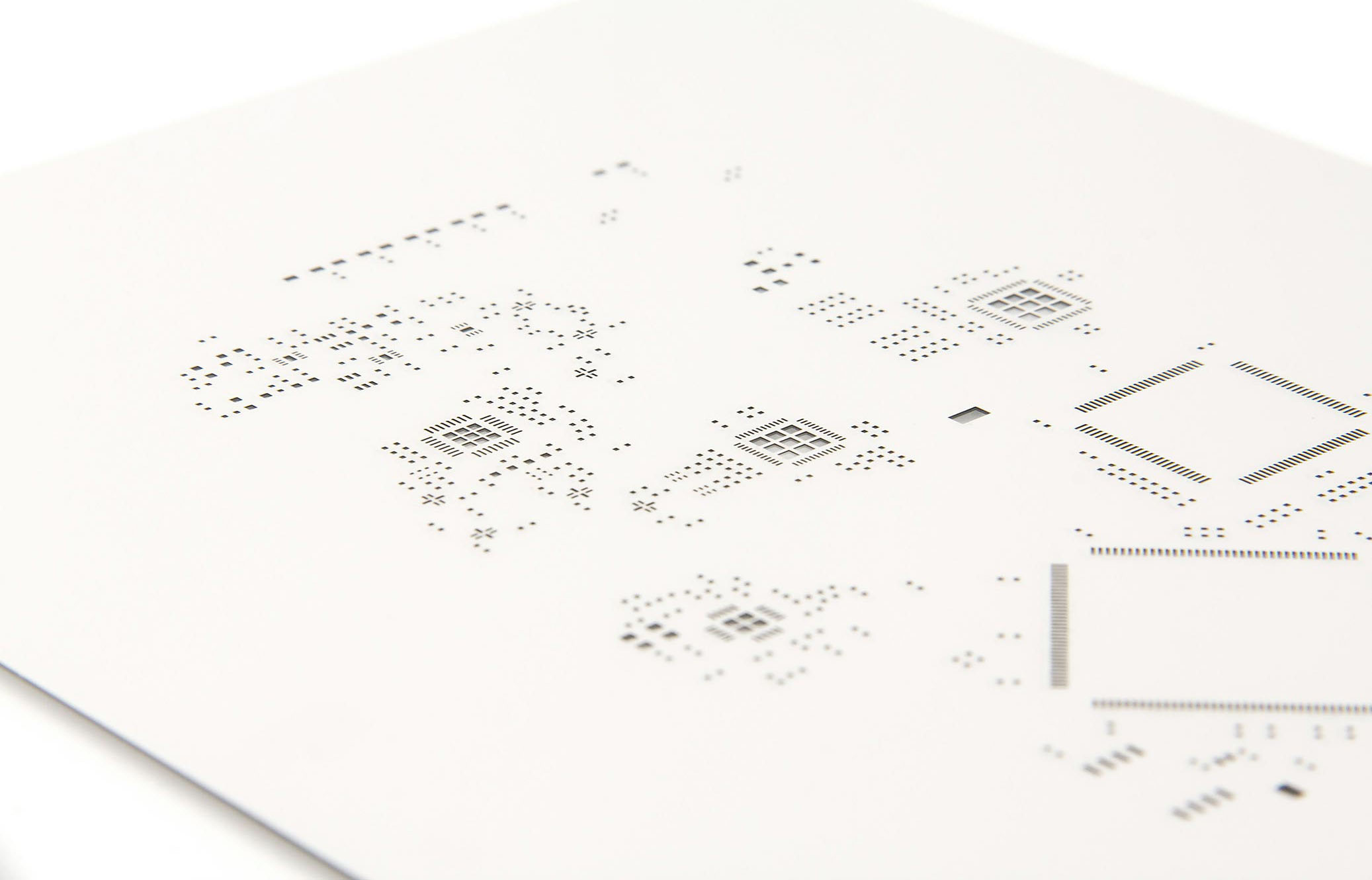
PCB SMT Stencil ,the unique goal is to move solder paste to the bare Printed Circuit Board.
PCB Stencil , SMT Stencil, SMD Stencil , Laser Stencil , What is it?
Apart from all types of Printed Circuit Boards (PCBs) such as Prototype PCB , Aluminum PCB , HDI PCB , Flexible PCB , Rigid Flex PCB , Thick Copper PCB, High TG PCB , JHYPCB also manufactures solder paste stencils to meet Surface Mount Technology (SMT) requirements.
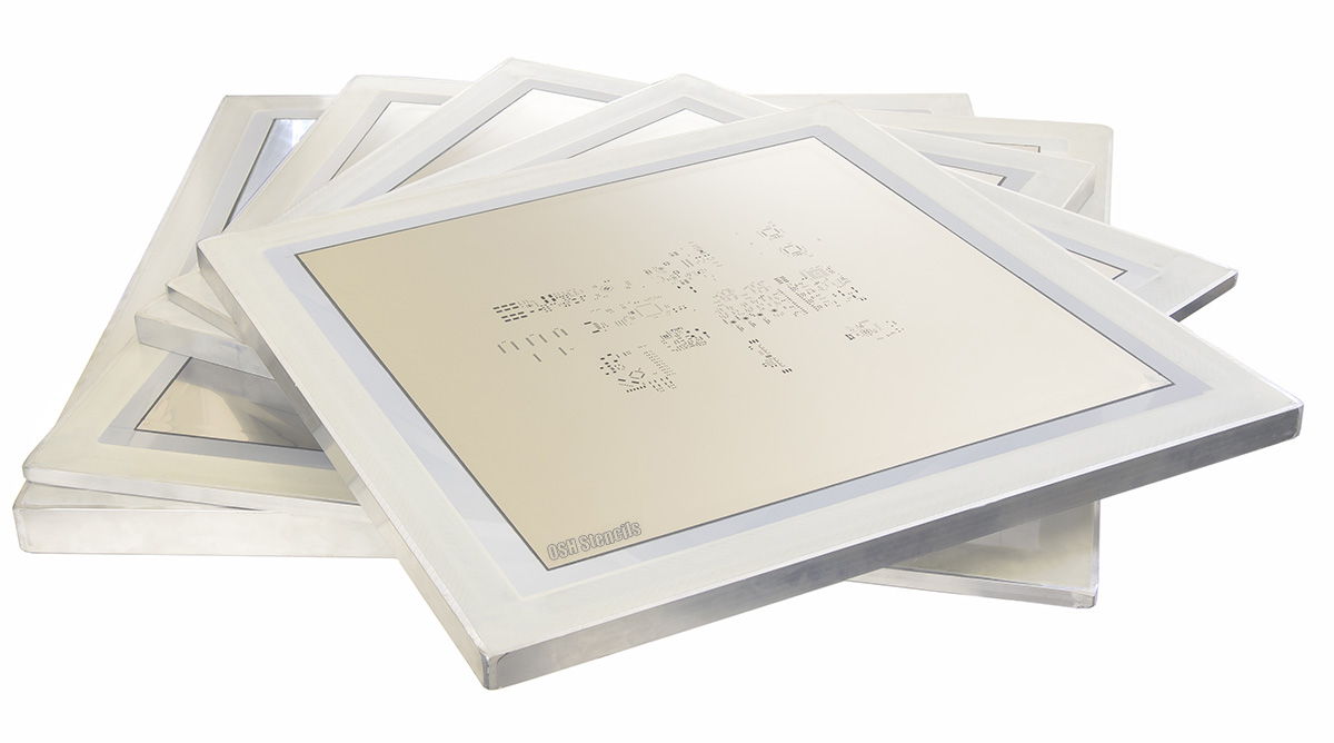
PCB Stencils, also called SMT stencils, SMD stencil, play a key role in transferring accurate amount of solder paste to correct positions on bare circuit boards ready for assembly. In other words, stencils can fast and efficiently ensure the most accurate solder paste amount and optimal electrical connection. With solder stencils, it is possible to use metal squeegee blades to apply solder paste easily over the openings on PCBs and make stencil to be well aligned with the surface of the advanced circuit board.
All of our SMT Stencils are 100% laser-cut type 304 full-hard stainless steel, ensuring the finest quality finish on the market today. We use a .001" laser beam with 98% overlap creating an extremely smooth hole that provides the best paste release. Most stencil fabricators use a .003" laser leaving mouse bites on the aperture edge. You can choose a PCB Prototype stencil, a frameless foil stencil, or a rigid permanently mounted stencil. Both the frameless and framed stencils come in various sizes to accommodate your printer and stencil requirements.
PCB Stencil Types Available:
1. Laser-cut stencils
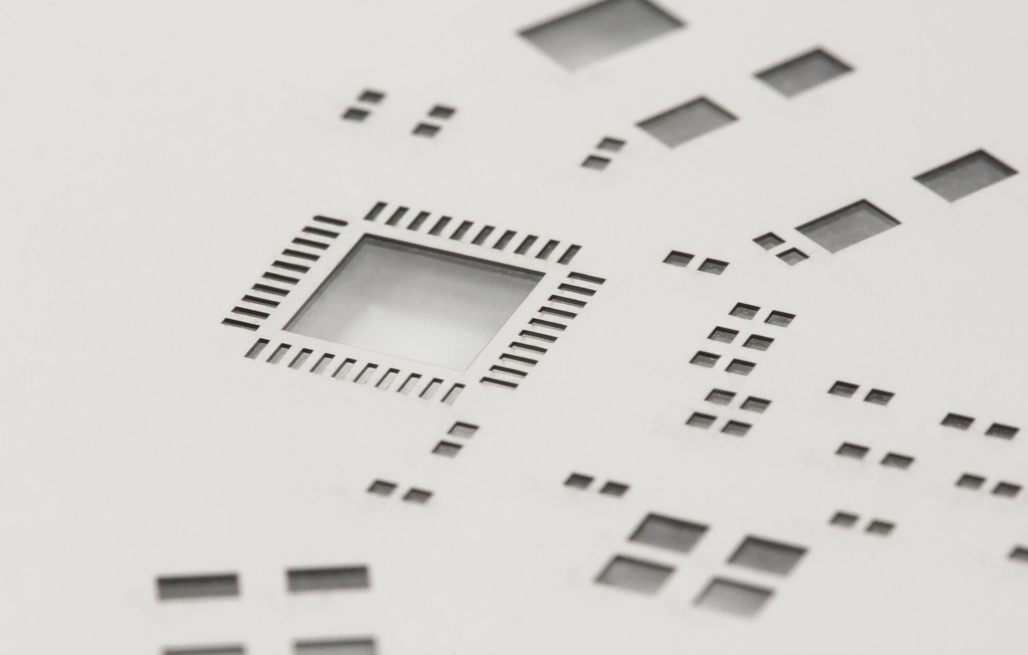
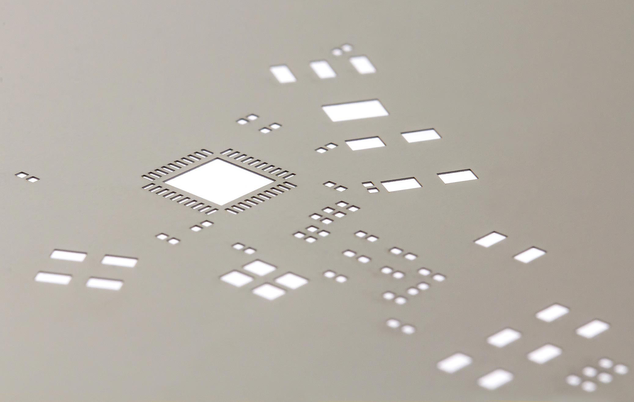
The openings are lasered on 100% stainless steel. Generally speaking, this kind of stencil can be produced with high quality and a high degree of precision within a short time.
- Advantages: high accuracy; barely influenced by objective elements; trapezoid opening beneficial for demoulding; suitable for accurate cutting; reasonable price;
- Disadvantages: relative low manufacturing speed.
2. Chemical-etch stencil
The openings are etched into the metal using acid. Usually this kind of stencil offers better protection on material temper and hardness.
- Advantages: one-time formation; relatively high manufacturing speed; low cost;
- Disadvantages: tending to form sand clock shape or large openings; numerous manufacturing stages and accumulating errors; unsuitable for fine pitch stencils; bad for environmental protection.
3. Prototype PCB Stencil (Low-volume manual printing. Ideal for prototypes)
When prototyping dictates fast action with minimal cost, our prototype stencils are the best solution. Prototype Stencils gives you a quality stencil and framework so you can handle assembly from the convenience of your own desk.
Prototype SMT Stencil Features:
- Eliminate the registration difficulty associated in hand printing with a flat piece of metal
- Eliminate printer set up for short run prototypes
- Allow quick alignment for repeatability
- Save money over full size stencils designed for automated printers<
- Squeegee included
| Prototype SMT Stencil Specs: | |
| Technology | 100% laser cut |
| Material Used | Stainless Steel |
| Stencil Thickness | 0.06 ~ 0.3 mm |
| Minimum Cut Width | 0.05 mm |
| Maximum Size | 736 X736 mm |
| Aperture Tolerance | within 0.007mm |
| Allow for Fiducial Data | Yes |
| Delivery | 1 ~2 Day |
4. NEW Prototype PCB Stencil Kit (with leaded or lead/free solderpaste)
Includes Prototype Stencil, one board holder, leaded or lead-free solder paste (must specify), temperature marker, squeegee, ESK-safe gloves and alcohol wipe.
5. NEW Pick and Place Tool
Handy and convenient for low quantity prototype assembly using the Prototype Stencils. Re-usable, includes vacuum bulb and vacuum clips with diameters of 3/8", 1/4", and 1/8".
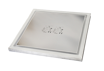
6. Framed SMT Stencils (Also called "Glue-in" or Mounted Stencils)
Framed stencils are laser-cut stencils designed for high volume screen-printing. With a framed stencil, your stencil is securely mounted to either a cast or extruded aluminum stencil frame a stencil frame using a mesh border, allowing for complete control.
Framed SMT Stencil Features:
- Unique Process for smooth aperture walls
- ery clean laser-cut apertures
- Excellent print performance
- Excellent for high-volume stencil printing on printed circuit boards
- Unique process creates permanent non-removable non-fading fiducial
- All framed SMT stencils are double bonded to extreme wear
- 24-hour turnaround standard
| Framed SMT Stencil Specs: | |
| Technology | 100% laser cut |
| Material Used | Stainless Steel |
| Frame Types | Cast, Space Saver |
| Stencil Thickness | 0.06 ~ 0.3 mm |
| Minimum Cut Width | 0.05 mm |
| Maximum Size | 736 X736 mm |
| Aperture Tolerance | within 0.007mm |
| Allow for Fiducial Data | Yes |
| Allow for Panelized Data | Yes |
| Delivery | 1 ~2 Day |
Framed PCB Stencil Specification
|
Framed PCB Stencil Area |
Maximum Squeegee Area |
|
300mm*400mm (11.81inch*15.75inch) |
120mm*220mm (4.72inch*8.66inch) |
|
370mm*470mm (14.57inch*18.5inch) |
200mm*300mm (7.87inch*11.81inch) |
|
400mm*600mm (15.75inch*23.62inch) |
220mm*400mm (8.66inch*15.75inch) |
|
400mm*700mm (15.75inch*27.56inch) |
220mm*500mm (8.66inch*19.69inch) |
|
400mm*800mm (15.75inch*31.5inch) |
220mm*600mm (8.66inch*23.62inch) |
|
400mm*900mm (15.75inch*35.43inch) |
220mm*700mm (8.66inch*27.56inch) |
|
400mm*1000mm (15.75inch*39.37inch) |
220mm*800mm (8.66inch*31.5inch) |
|
400mm*1200mm (15.75inch*47.24inch) |
220mm*1000mm (8.66inch*39.37inch) |
|
400mm*1400mm (15.75inch*55.12inch) |
220mm*1200mm (8.66inch*47.24inch) |
|
420mm*520mm (16.54inch*20.47inch) |
240mm*340mm (9.45inch*13.39inch) |
|
450mm*550mm (17.72inch*21.65inch) |
270mm*370mm (10.63inch*14.57inch) |
|
500mm*800mm (19.69inch*31.5inch) |
320mm*600mm (12.6inch*23.62inch) |
|
500mm*1200mm (19.69inch*47.24inch) |
320mm*1000mm (12.6inch*39.37inch) |
|
550mm*650mm (21.65inch*25.59inch) |
340mm*440mm (13.39inch*17.32inch) |
|
584mm*584mm (23inch*23inch) |
380mm*380mm (15inch*15inch) |
|
736mm*736mm (29inch*29inch) |
480mm*480mm (19inch*19inch) |
7. Frameless SMT Stencil - Foil/Plate Only (for universal frames)
Foil or Plate Only stencils are designed to work within interchangeable plate or "universal" systems. Also referred to as "reusable", these stencils do not need to be permanently glued into a frame.
Frameless SMT Stencils also referred to as foils are laser cut solder paste stencils designed to work with stencil tensioning systems known as reusable stencil frames. This type of stencil does not need to be permanently glued in a frame. Frameless stencils are significantly less expensive than framed stencils and provide money-saving storage while still delivering superior quality and performance.
Frameless SMT Stencil Features:
- Reduced storage space requirements
- Significantly less expensive than framed stencils
- Excellent for prototype Printed Circuit Board Assembly or short runs
- Smooth aperture walls, can be used for 16 Mil pitch and below and for Micro BGA's
- 24-hour turnaround standard
| Frameless SMT Stencil Specs: | |
| Technology | 100% laser cut |
| Material Used | Stainless Steel |
| Stencil Thickness | 0.06 ~ 0.3 mm |
| Minimum Cut Width | 0.05 mm |
| Maximum Size | 280 X 380 mm |
| Allow for Fiducial Data | Yes |
| Allow for Panelized Data | Yes |
| Delivery | 1 ~2 Day |
8. Frameless SMT Stencil - Foil/Plate Only (for hand printing)
For times when you need precise control for smaller production runs, our Foil or Plate Only stencils are ideal. These frameless stencils allow you to hand print with precision just the amount you need and can be stored conveniently.
9. Electroformed SMT Stencils
Electroformed SMT stencils are nickel-based, electroform foils permanently mounted in a stencil frame using a mesh border to tightly stretch the stencil foil taut in the frame. Electroformed stencils offer the best paste release characteristics available and are frequently used for fine pitch (20 mil to 12 mil pitch) SMT applications on printed circuit boards. They are also used for µBGA's, Flip Chip, and Wafer Bumping (12 mil to 6 mil pitch).
Electroformed SMT Stencil Features:
- The smooth trapezoidal sidewalls of an electroformed stencil allow for better paste release
- Nickel has a lower coefficient of friction compared to stainless steel
- Electroform foils are harder than full hard stainless steel of comparable thickness, providing for longer stencil life
- 24-hour turnaround standard
| Electroformed SMT Stencil Specs: | |
| Technology | Electroforming |
| Material Used | Nickel |
| Suitable Applications | All Component Pitches |
| Aperture Tolerance | within 0.007mm |
| Stencil Thickness | 0.06 ~ 0.3 mm |
| 0.06mm.0.08mm.0.1mm.0.12mm.0.13mm.0.15mm.0.18mm.0.2mm.0.3mm | |
| Positional Accuracy | ± 0.008mm |
| Delivery | 1 ~2 Day |
What's the difference between a framed stencil and a frameless stencil?
A framed PCB stencil will have a 0.5" to 1.5" thick metal frame around it, similar to a picture frame. Framed stencils are often used by contract manufacturers, assembly and board houses, and large scale production facilities and are commonly placed in a manual or automated stencil printing machine. Frameless stencils are a thin sheet of material cut with a small border around your design. For example pictures on these products, please visit our Gallery.
What's the difference between Polyimide and Stainless Steel?
All stencils are made with high quality Polyimide and Stainless Steel. We use only the industry leading Stainless Steel, designed specifically for stencils. These materials are ideal for prototype or Multilayer PCB .
Stainless Steel: 0.0007" Laser spot size, 0.001" minimum aperature size.
Polyimide Film: 0.003" Laser spot size, 0.005" minimum aperature size.
Polyimide has a lower precision rate due to the way it is processed and its ability to withstand heat during the cutting process. Minor variances will occur when the material reacts to the laser. Paste release is great, but this material should be limited to a small number of uses and with components 0402 or bigger.
The minimum aperature size for Polyimide is 0.005" vs 0.001" for Stainless Steel. Polyimide also has a natural curl in the material caused by the way the film is manufacturered, this is outside of our control. Stainless Steel provides the ultimate in precision and quality, with a 0.0007" spot size, and exceptional paste release with a truly flat surface. If you want the absolute best reflow experience, there is no comparison, Stainless Steel is the superior material.
Analysis and Treatment of Common Problems in PCB SMT stencil
- Insufficient solder paste
- Smudging/bridging
- Misalignment print
- Bow and twist
How to Determine Stencil Size?
Stencil size is composed by two parts: internal size and overall size. Internal size is the size compatible with that of PCB ready to be assembled while overall size refers to the size compatible with printer parameter limit. As long as both sizes are accurately designed, stencil will be able to make full use of its functions.
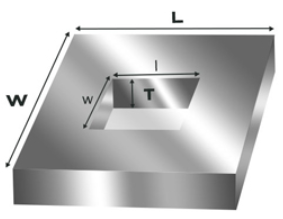
Internal size of stencil can be figured out conforming to the following rule:
- Width of Framed Stencil = width of PCB + 100mm while its Length = length of PCB + 100mm
- Width of Frameless stencil = width of PCB + 200mm while its Length = length of PCB + 200mm
For example, if one circuit board size is 50*50mm, then the size of its framed stencil should be around 150*150mm and the size of its frameless stencil should be around 250*250 mm.
It's easy to remember and operate so it worked for manual solder paste printing in SMT assembly prior to the advent of automatic printer. It can be said that different PCB sizes lead to generations of different internal sizes of stencil.
When it comes to automatic solder paste printer, however, it's relatively solid. Overall size of stencil has to be determined by parameter limit of the equipment, that is, printer, because stencil has to work within the range of printer with a frame. Different printers feature different parameter regulations. As far as PCBCart is concerned, the stencil size compatible with our printer can be either 650mm*650mm or 736mm*736mm.
PCB designers have to focus on internal size of stencil, they don't need to care about its overall size since it is generally determined by the parameters of printer in your contract assembler workshop.
How to Use PCB SMT Stencils?
PCB Stencil
PCB Stencil,SMT Stencil,SMD Stencil,Laser Stencil
JingHongYi PCB (HK) Co., Limited , https://www.pcbjhy.com