PXI bus is a new generation instrument bus developed by NI based on computer peripheral bus PCI. It has become the standard of open bus in the industry. The digitizer module based on PXI bus is an important data recording and processing in modern test system. equipment. Design a dual-channel 12-bit/250 MHz sampling frequency high-speed digitizer module with high-performance FPGA devices as the core to achieve high-speed A/D control and high-speed data processing and storage, solving the problem of long-term high-speed recording signal testing .
1 System working principle
The digitizer module is mainly composed of front-end signal conditioning path, analog-to-digital conversion circuit, data storage unit, data acquisition control circuit, PXI interface circuit, etc. The principle block diagram is shown in Figure 1.
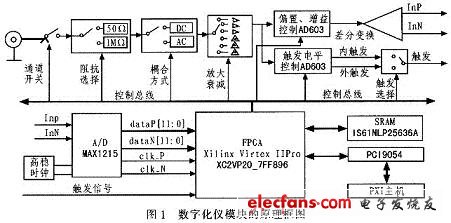
The high-speed analog signal is first processed through the signal conditioning path for amplification, attenuation, etc., and the amplitude is adjusted to the voltage range allowed by the A/D converter, and converted into a differential signal of the LVDS format, and then sent to the A/D converter; The chip receives the high-speed data stream of the A/D output, and after being processed by the speed reduction, decimation filtering, etc., is stored in the data storage unit SRAM, and sends an interrupt signal, and the PXI host reads the data stored in the SRAM via the FPGA after responding to the interrupt. Host memory, complete subsequent data processing and display. The PXI host sends control commands through the PXI bus, and realizes data acquisition and conditioning path control through FPGA decoding. The digitizer module reserves 4Mb of storage capacity per channel. When composing a PXI test system, data can be written to the computer's hard disk for longer recording. The two channels can work independently or in association with each other. The acquisition mode can have multiple modes such as internal trigger, external trigger, software trigger, and channel trigger.
2 system design and implementation
2.1 Modular FPGA design
The digitizer designed in this paper is based on high-performance FPGA chip. FPGA bears most of the control and data processing tasks and is the core device of this design. Modular design of FPGAs is a common method for large-scale system design. Reasonable splitting of functional modules can speed up the development of FPGAs and facilitate the porting and reuse of code. At the time of design, the FPGA is divided into high-speed A/D interface module, data deceleration module, conditioning path control module, storage interface module, PXI interface control module and other main functional module design. FPGA internal module partitioning and data flow are shown in Figure 2.
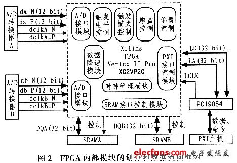
The A/D interface module mainly realizes the interconnection of the FPGA and the high-speed A/D converter, and receives the data and the sampling clock in the LVDS format bus. The part of the circuit determines the stability of the data acquisition, and needs to be guaranteed from both hardware and software; The speed module uses a decimation filter to reduce the signal to the required sampling rate; the conditioning path control module mainly controls the A/D front-end circuit, including coupling mode, matched impedance selection, gain automatic control, offset and trigger level control, etc. The PXI interface part mainly realizes the communication decoding with the PXI host; the storage control module completes the control of the external SRAM to realize data buffering; the clock management module is responsible for the frequency division and frequency multiplication of the sampling clock.
2.2 High-speed data acquisition and storage interface design
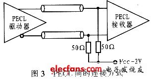
The design of the input and output interface of the high-speed data acquisition system is particularly important. The interconnection of high-speed IC chips is one of the key factors determining the stability of the data acquisition system. Low power consumption and high signal-to-noise ratio are the main problems to be solved. There are two interfaces for inter-chip interconnects in high-speed acquisition systems: PECL and LVDS. The positive voltage emitter-coupled logic PECL (PosiTIve Emit-ter-Coupled Logic) signal has a small swing and is suitable for serial or parallel connection of high-speed data. The connection between PECL is generally DC-coupled, and the output is designed to drive a 50 Ω load to (VCC -2V), the connection circuit is shown in Figure 3.
The Low Voltage Different Signal (LVDS) standard is a small amplitude differential signaling technique that uses very low amplitude signals (100 to 450 mV). Transfer data through a pair of parallel PCB traces or balanced cables. The current flowing through the two parallel differential signal lines is opposite in direction, the noise signal is coupled to both lines at the same time, and the receiving end only cares about the difference between the two signals, so the noise is cancelled. Since the electromagnetic fields around the two signal lines also cancel each other, the differential signal transmission is much smaller than the single-line signal transmission electromagnetic radiation, thereby improving transmission efficiency and reducing power consumption. The input and output of LVDS are internally matched, and the direct connection mode can be used. The connection mode is shown in Figure 4.

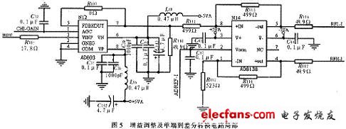
In this design. The A/D converter uses Mamix's MAXl215, a 12-bit/250 Ms/s high-speed A/D converter with excellent SNR and SFDR characteristics, using a 250 MHz differential sampling clock to receive differential inputs. The signal outputs a differential digital signal in 12-bit LVDS format to provide a differential synchronous clock signal. In order to improve the test accuracy, the single-ended input signal needs to be converted into differential mode and then sent to A/D. The gain adjustment and the single-ended to differential conversion circuit are shown in Figure 5. Considering the impedance matching problem, when the single-ended signal is converted to the differential mode, a 50 Ω matching resistor needs to be connected in series on the two differential lines as the transmitting end of the LVDS signal.
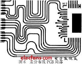
In the design of the PCB, special processing is required for the differential lines. The actual wiring tolerance of the differential line within the routing interval should be controlled within 5 mils; the distance between the two lines within the differential pair should be as small as possible to allow external interference to be common mode; to ensure that each differential pair The lengths match each other to reduce signal distortion; the power layer is used as the signal loop of the differential line, because the power plane has the minimum transmission impedance, which can effectively reduce the noise effect. Figure 6 shows a portion of the design PCB.
In this design, the FPGA as the receiving end of the LVDS signal first needs to convert the LVDS differential data and the synchronous clock signal of the A/D input into a single signal. Here, xilinx's Virtex II-Pro series FPGA is selected. This series of FPGAs embed high-speed I/O interfaces, which can realize ultra-high bandwidth system chip design, support LVDS, LVPECL and other differential interfaces, and has strong adaptability. Provides a complete solution for high speed data interfaces. The reception of the LVDS differential signal can be realized by instantiating the IBUFDS_LVDS module, and the internal matching resistor is used in the program to achieve impedance matching of the LVDS. The differential clock signal is connected to the FPGA by the global clock input pin, and then the clock is converted into a single signal by the xDSP-specific digital clock management module (DCM), and the frequency division and shift equalization processing is performed as a clock signal for subsequent processing.
2.3 PXI interface design
PXI is an extension of PCI in the field of instrumentation (PCI eXtensions for InstrumentaTIon), which develops the PCI bus technology defined by the CompactPCI specification into mechanical, electrical and software specifications for test, measurement and data acquisition applications, thus forming a new virtual Instrument architecture. The PXI modular instrumentation system delivers high-speed performance and compatibility with PCI, forming a mainstream virtual instrumentation test platform. This design uses PCI9054 for PXI interface hardware design. PCI9054 is a 32-bit/33 MHz universal PCI bus controller special device produced by PLX Company of USA. It has powerful functions and simple user interface for PCI bus interface. Development provides an easy way.
2.4 PXI driver development
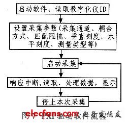
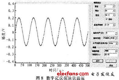
PXI's software requirements include support for standard operating system frameworks such as Microsoft Windows NT and 95 (WIN32), requiring all instrument modules with configuration information (configuraTIon information) and industry-standard development environments that support standards (such as NI LabVIEW, LabWindows/CVI, and Microsoft's VC/C++, VB, and Borland's C++, etc., and VISA-compliant device drivers (WIN32 device drivers). This design uses KRF-Tech's Windriver to write device drivers. Windriver has written API function packages for PLX and AMCC dedicated interface devices, which reduces the development difficulty. The software flow chart of the driver is shown in Figure 7. Figure 8 is the interface of the digitizer module soft panel. All control of the digitizer can be done by setting the virtual software interface.
3 Conclusion
This paper presents the design and implementation method of high-speed digitizer module based on PXI bus interface. It introduces the LVDS interface, LVPECL interface circuit structure and connection method in high-speed data acquisition system, and is applied in the designed digitizer module. The system can operate stably at 250 MHz for high-accuracy, long-term data acquisition and analysis. The digitizer module has been successfully applied to multiple PXI test systems and is widely used in industrial automation, communications, scientific research, military, aerospace, consumer electronics and other fields.
Guangzhou Yunge Tianhong Electronic Technology Co., Ltd , https://www.e-cigarettesfactory.com