In the near future, automotive radar systems will become more and more popular, and they provide many comfortable and safe applications. Short-range radars range from a few centimeters to 30 meters and can be used for blind spot detection, reversing assistance or parking space measurements to guide car self-parking. The long-range radar can reach 250 meters and is used to start adaptive cruise control to keep the car and front speed consistent. In addition, it can activate more important functions such as collision warning, emergency braking, and even impact warning detection systems, which may trigger seat belt tension meters or other active or passive safety functions. Obviously, with these latter functions, the electronic control system needs to achieve the highest level of functional safety, because this system will eventually turn or brake the car without driver intervention.
This article refers to the address: http://
The development and innovation of this radar technology is continuously applied in other applications such as mobile industrial computers, cranes, factory safety equipment, etc., and this application field requires strict security protection. Coupled radar and machine vision can also create a powerful combination that complements each other to create a more accurate and reliable system. When machine vision is blocked, the radar can operate in rain, fog and dirt. In addition, the radar can further extend its detection range and detect events in the indirect line of sight. A system that combines machine vision with radar and some smart sensor fusion algorithms can take advantage of the benefits of these two sensing technologies.
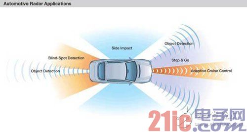
Figure 1: Automotive radar application
77 GHz radar technology
In the collision warning system, the signal from the 77 GHz transmitter will be reflected by objects in front of the body and then captured by multiple receivers distributed throughout the body. The transmitter emits a frequency modulated continuous wave signal, that is, in a fixed period of time, the frequency varies up and down with a typical triangular wave signal. Since radio waves propagate at a constant speed of light, the propagation distance can be calculated by measuring the frequency difference between the transmitted wave and the received wave (i.e., the slope of the frequency as a function of time). The velocity measurement uses the Doppler effect, that is, the observed reflected signal frequency is different from the emitted frequency.
The radar system is not a new highlight. The new highlight is that automakers want to build this system into midsize cars in the last few years, so the system must be low-cost, high-quality. This means a big shift from expensive professional radar systems to standard automotive equipment types. The challenge is to reduce the cost while actually improving the quality of the product and reducing the number of parts per million pieces. This shift is shown in the “Quality and Cost Marketing Value Mapâ€.
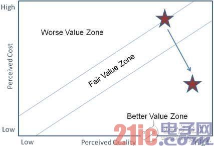
Figure 2: Marketing Value Map
This marketing value map shows the transition from a high-cost, good-quality system to a low-cost, higher-quality system. In order to achieve this goal, we must deal with many challenges.
Radar cost and quality challenges
Conventional radar uses a rotating antenna. This is also the principle of object space mapping. This may be suitable for large systems with expensive control systems, but certainly not for automotive mass production. One solution to eliminate rotating antennas is to use phased arrays or patch antennas for multi-channel transmit and receive channels. The air separation antenna will receive a reflected signal with a slight time difference. This difference is then used to reconstruct the position of the object without moving the antenna. A disadvantage of such a patch antenna is that multiple transmit and receive channels are required to connect the antenna. A typical system will employ four similar transmit antennas and 16 receive antennas. However, from an economic point of view, it is not feasible to repeat 16 receiving circuits and 4 transmitting circuits.
Then another innovation comes in handy. Instead of using RF differential circuits, Freescale has developed a dedicated RF BiCMOS process that is capable of integrating 77 GHz RF circuits onto a single chip. Beginning with the development of the high-performance SiGe:C (silicon germanium carbon) 180nm process, Freescale has also developed a dedicated 300GHz Fmax RF transistor capable of processing 77GHz radar signals on the chip. Combined with analog and digital CMOS circuits, this process supports full integration of multi-channel 77GHz system-on-chip. Therefore, on-chip integration can offset multi-channel overhead costs.
Advanced packaging technology
Having a 77 GHz solid-state silicon process is a huge asset, but processing and reporting it on a printed circuit board is another challenge. Traditional package parasitic impedances can destroy signal information at high frequencies. One way to deal with this problem is to solder bare chips to a dedicated PCB using precision wire bonding techniques instead of using typical packages and higher cost wave soldering techniques. The new advanced packaging technology called "RCP (Reassignment Chip Package)" comes in handy.
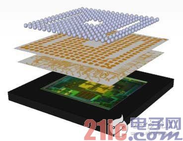
Figure 3: Layers in the RCP package
RCP uses a thick lithography technique instead of a PCB-type material to mount a copper interconnect layer on a chip or multi-chip system. This substrateless packaging technology has lower capacitance and inductance parasitic behavior. High-frequency signals can be routed at 77 GHz through this package with acceptable performance compared to the bare die soldering process. The advantage is that the complete set of tools for conventional PCBs can be used to solder this part, which means low cost processing.
With this process and packaging technology, Freescale continues to design integrated transmitter and receiver radar circuits.
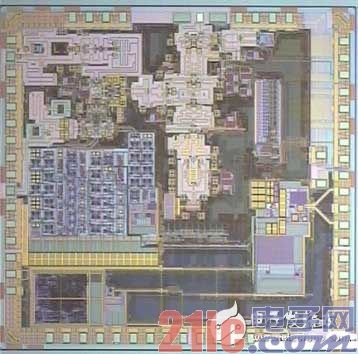
Figure 4: 77 GHz radar transmitter bare chip
The transmitter integrates a 77 GHz frequency synthesizer, a half-frequency voltage-controlled oscillator, a 10 GHz cross-link phase-locked loop, a power amplifier, and a 28-bit sigma-delta modulator. This is accompanied by specific ESD protection (RF and DC) and digital control via the SPI interface.
At the receiving end, we integrated a typical four receive channels and a local oscillator at 38 GHz, as well as an output differential IF. A typical noise figure of 13dB is achieved without the need for a low noise amplifier. This helps maintain low power consumption and high linearity.
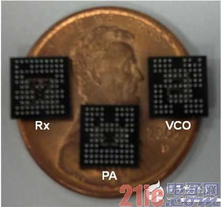
Figure 5: RCP-packaged radar chipset functional safety microcontroller
The microcontroller is used to control the RF radar transmitter and process the data from the receiver. Functional safety microcontrollers are required if the critical safety nature of the application is taken into account. The challenge for system engineers is to build systems that need to be able to prevent dangerous failures or at least effectively control in the event of a failure. Dangerous failures can result from random hardware failures, system hardware failures, and system software failures.
The functional safety standard IEC 61508 and the automotive-appropriate ISO 26262 standard are suitable for ensuring that electronic systems in general industrial and automotive applications are completely safe. The IEC 61508 standard defines four full safety integrity levels (SIL), with SIL 4 representing the most stringent safety level. The ISO standard defines four automotive safety integrity levels (ASIL), of which ASIL D represents the most stringent safety level. Each level corresponds to a range of possible targets for a safety function failure.
There is no direct correspondence between SIL and ASIL levels, but ISO 26262 pushes security processes and requirements to a deeper level. At the beginning of the design process, it is necessary to collect credentials to prove that the product was developed according to standards. Any potential deviations found must be recorded to ensure adequate rescue measures can be taken.
They use different methods to implement a secure microcontroller. The traditional approach is to use two separate microcontrollers to replicate software on completely different controllers. The same software can be run on each microcontroller and the results are compared. If the results are the same, everything is fine; if it is not the same, then the system knows that there is an error, or resolves it and/or puts the system into a safe state. Another option is that one microcontroller can only run security software and monitor another microcontroller that is running the application.
With a separate microcontroller, the system must be designed and implemented from the start.
In contrast, pre-certified microcontrollers are now available. These solutions primarily detect and reduce single points of failure, potential failures, and non-independent failures. This is achieved through built-in security features in microcontrollers, power management ICs and sensors, including self-test, monitoring and hardware-based redundancy. For microcontrollers, the on-chip redundancy provided is for the following key components, such as:
- Multiple CPU compute cores with delayed lockstep
- I/O processor core
- Direct memory access controller
- Interrupt controller
- Double crossbar switching bus system
- Memory protection unit
- Fault collection unit
- Flash memory and RAM controller
- peripheral bus bridge
- System and watchdog timer
- and end-to-end error correction code
The main advantage of the data replication field is the function of the MCU, which can detect single-point faults such as soft errors that occur more frequently, not only detecting errors in the kernel but also detecting critical sub-modules.
A built-in self-test (BIST) mechanism is provided for the core, memory, crossbars, communication modules, and peripherals. In addition, the device is optimized to prevent common cause failures caused by clock or voltage supply problems. The MCU provides hardware blocks that detect clock skew and hardware monitoring of the main voltage, such as internal core voltage and flash supply voltage.
Dual-core lock-step MCUs do not reduce the need to implement security measures at the software and system levels, such as monitoring the output values ​​of software path calculations very independently. However, in other aspects of higher integration, these MCUs do not provide separation of concerns for verification. In a solution based on multiple single core MCUs, the ability to detect and control random hardware failures is highly dependent on the software.
Dual-core lock-step MCUs can verify and validate key functional security attributes of a computing infrastructure at a software-independent hardware level, since the computing infrastructure is provided in an integrated form, which also represents an integrated security mechanism. This is a significant benefit in the hardware and software co-design process. In addition, separation of concerns facilitates rapid location problems. If the security mechanism for monitoring dual-core locksteps is triggered, the cause may be attributed to a hardware-level random hardware failure, and if software monitoring is triggered, the cause may be due to a system-level failure or a systemic failure in the software.
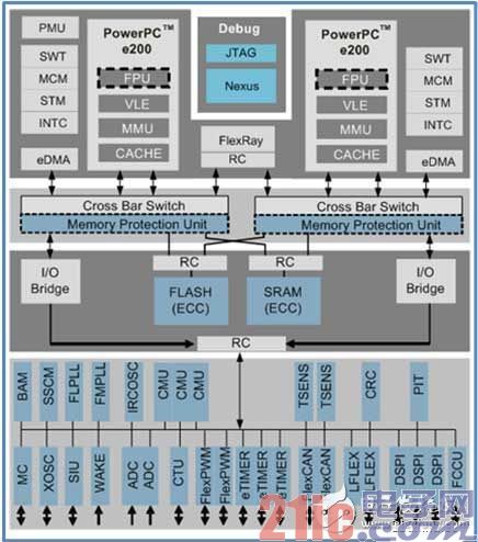
Figure 6: Dual-core lock-step MCU structure
The dual-core lock-step MCU approach provides a potential usability advantage. In modern MCUs, the kernel area is getting smaller and smaller, much lower than 5% of the entire MCU, and the MCU as a whole is usually assigned a probability of random hardware failure (PMHF) of about 1%. Therefore, the kernel accounted for approximately 0.05% of the area at first. However, the correct operation of the kernel must be ensured in order to implement forward recovery techniques in the software to resolve the remaining 99.95% of the factors affecting PMHF and to ensure system availability. In addition, dual-core lockstep MCUs provide the appropriate infrastructure to implement multiple, sufficiently independent channels.
Functional safety accessory
To support a complete system solution for functional safety applications, Freescale has developed a complementary power system base chip (SBC) that combines both security monitoring and power generation for MCUs.
These SBC devices power the MCU and other system loads and optimize power consumption through a low-power, power-saving mode. In addition, they usually integrate physical layer interfaces and serial peripheral interfaces, using MCU for control and diagnostics. The combination of the MCU and the analog system base chip can be viewed as a single SEooC (Independent Security Unit), which facilitates evaluation of system security. This architecture reduces the number of system-level components, meets functional security requirements, and enhances reliability. Take four security measures to ensure interaction between the MCU and the SBC:
- ups
- Fail-safe input monitoring key signals
- Fail-safe output drive fail-safe status
- Watchdog for advanced clock monitoring
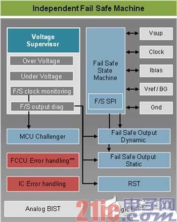
Figure 7: SBC fail-safe machine
When combined with an MCU, each security measure can be optimized to achieve the highest level of security performance. At the system level, the security check mechanism proposed by the MCU can be monitored by the SBC device through the bistable protocol of the Fault Acquisition Control Unit (FCCU). This type of IC cross-check, such as query timing monitoring, allows external detection of the system as an additional measure to further ensure fault detection. In order to comply with the safety architecture of the system-based chip family, redundant paths can be provided for safety state activation via a dedicated fail-safe output. When a fault condition occurs, these outputs set the application to a deterministic state to compensate for the MCU fail-safe output.
These hardware implementations help software engineers simplify the software architecture and implement software development strategies that focus on using a single MCU approach to ensure security.
System and chipset compliance
Functional safety compliance is achieved at the system level and is the responsibility of the system designer. The MCU and SBC chipsets are designed separately from the final application, such as parking systems, advanced driver assistance systems or mobile cranes. Thus, the chipset can be considered as a SEooC for development. SEooC is a safety-related component developed rather than in the context of feature vehicle functionality or end-use applications. We developed SEooC components that conform to the ISO26262 standard in accordance with custom guidelines.
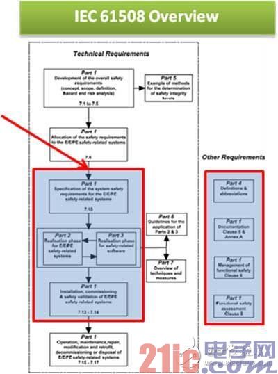
Figure 8: Chipset IEC Scope
Freescale has consolidated its measures to support the functional safety needs of the SafeAssure brand market. It covers security support, security hardware, security software, and security processes to ensure that these aspects are fully covered during the development phase of each product. Typical deliverables will include:
- Security Architecture Analysis: FMEDA, CCA or FTA
- User Guide: Safety Manual, Safety Application Note
- Development process evidence: PPAP, security plans and certificates
The aim is to reduce the time and complexity of developing safety systems in accordance with ISO 26262 and IEC 61508 and to simplify the system compliance process, which meets the requirements of specific automotive and industrial functional safety standards.
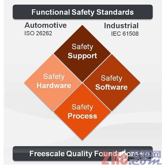
Figure 9: Freescale Security Plan
Heating Eye Mask,Self-warming Eye Mask,Portable Heating Eye Mask,Rechargeable Heating Eye Mask
Ningbo Sinco Industrial & Trading Co., Ltd. , https://www.newsinco.com