Field programmable gate arrays, or FPGAs, are further developed based on programmable devices such as EPLD, PAL, and GAL. As an semi-custom circuit in the field of professional integrated circuits, FPGAs not only solve the shortcomings of custom circuits, but also overcome the shortcomings of the original programmable devices due to the limited number of gates. The use of FPGAs is very flexible, and the same FPGA can achieve different circuit functions by using different programs. FPGAs are now widely used in communications, instrumentation, networking, data processing, industrial control, military, and aerospace. With the further reduction in cost and power consumption, FPGAs will be used in more fields. The design of the motor-based speed measurement system based on FPGA is based on the Quartus II design platform, using the hardware description language VHDL and modular design, and dynamically displaying the measurement results through the digital tube drive circuit. This design has the characteristics of less peripheral circuits, high integration, and high reliability, which can be used to measure the motor speed value.
Peripheral circuit design
The sensor converts the analog signal of the motor speed into a digital pulse signal and sends it to the FPGA module. At the same time, the accurate clock signal generated by the reference clock circuit and the reset signal generated by the reset circuit are sent to the FPGA module. The FPGA module generates a frequency dividing circuit, a decimal counter circuit, a data processing circuit, and a display decoding circuit. The reference clock signal sent by the frequency dividing circuit is divided to obtain a gate signal as an enable signal of the decimal counter. The function of the data processing circuit is to process the data obtained by the decimal counter and then send it to the display decoding circuit for conversion and decoding. The overall block diagram of the motor speed measurement system is shown in Figure 1. The peripheral circuits are divided into: a reference time base circuit, a reset circuit, a sensor measurement circuit, and a display circuit.

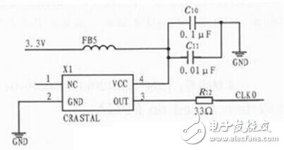
Figure 2 Active crystal oscillator circuit diagram
Reference time base circuit design
The reference time base circuit uses a 50 MHz active crystal oscillator. The 3.3 V power supply is connected to the VCC port of the active crystal through FB5, and the high frequency interference signal is filtered through C10 and C11. A 50 MHz clock signal is output from the OUT port. The crystal oscillator circuit is shown in Figure 2.
Reset button design
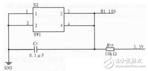
Buttons are commonly used as interfaces for human-computer interaction in embedded intelligent control systems. We usually input various information to the system through buttons, adjust various parameters or issue control commands. The processing of buttons is a very important function module. The interaction performance of the entire system also affects the stability of the system. In this design, the manual reset of the FPGA module is realized by pressing the button. The reset button is shown in Figure 3.

Figure 3 reset button circuit diagram
Display circuit design
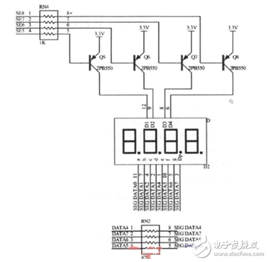
The display circuit we used in this design is shown in Figure 4.

It can be known from the digital tube display circuit that this is a common anode digital tube. When the low level is input to the bit selection terminals SE1 to SE4, the triode is turned on, and D1 to D4 are connected to the high level. From the a to the DP end, enter the digital tube display code, you can get the number we need, and let the digital tube select the conduction by the bit selection end.
This design is based on the FPGA motor speed measurement system design, using the Quartus II software developed by Altera Corporation as the design platform, which can measure the pulse signal converted by the sensor on the FPGA development board, and calculate the motor speed value by calculation. In this design, some extensions can be made. An alarm circuit can be added to set an alarm value. When the measured speed value is greater than this alarm value, the buzzer alarm or the digital tube can be illuminated.
Relative to LC To SC UPC Duplex,Optical fiber jumpers (also known as optical fiber connectors), that is, optical fiber connectors that are connected to optical modules, are also available in many types, and they cannot be used mutually. The SFP module is connected to the LC fiber optic connector, and the GBIC is connected to the SC fiber optic connector. The following is a detailed description of several commonly used optical fiber connectors in network engineering:
â‘ FC-type fiber jumper: The external strengthening method is a metal sleeve, and the fastening method is a turnbuckle. Generally used on the ODF side (most used on the distribution frame)
â‘¡SC type optical fiber jumper: the connector that connects to the GBIC optical module, its shell is rectangular, and the fastening method is a plug-in latch type, without rotation. (Most used on router switches)
â‘¢ST type optical fiber jumper: commonly used in optical fiber distribution frame, the shell is round, and the fastening method is turnbuckle. (For 10Base-F connection, the connector is usually ST type. Commonly used in optical fiber distribution frame)
â‘£LC-type optical fiber jumper: the connector for connecting the SFP module, which is made by the easy-to-operate modular jack (RJ) latch mechanism. (Router commonly used)
Lc To Sc Upc Duplex,Lc To Sc Upc Simples,Lc Upc To Sc Apc Simplex,Lc Upc To Sc Apc Duplex
Nanjing Jisu Shitong Technology Co., Ltd , https://www.netairs.com