Electronic design and simulation is the key content in the basic learning of electronic technology, and it is a key link to transform theoretical knowledge into practical ability. In this paper, for the experimental requirements of digital circuit comprehensive knowledge, the basketball game 24 s timer was designed and simulated by MulTIsim software.
1 design and circuit composition
The 24-second timer of basketball game is a simple application of digital circuit. In the design process, the circuit is divided into four parts: timing circuit, control circuit, display circuit and alarm circuit.
The design scheme block diagram is shown in Figure 1. The timing circuit and the control circuit are the main modules in the design, wherein the timing circuit is composed of a second pulse generator and a counter. The counter completes the 24 s timing function, and the control circuit mainly performs functions such as direct clearing of the counter, start counting, pause/continuous counting, and the like.

Figure 1 24-second timer design block diagram
In the design, combined with actual needs, the counter selects 74LS192 integrated chip, 74LS192 is a decimal programmable synchronous addition counter, which uses 8421 code decimal code, and has the functions of direct clearing, setting, adding and subtracting. The conversion of the hexadecimal is realized by the feedback terminal and the set terminal; the second pulse generator is composed of a 555 integrated circuit or a multivibrator composed of a TTL NAND gate. The display circuit consists of a 74LS48 decoder and a common cathode seven-segment LED display. The alarm circuit can be replaced by a light-emitting diode and a buzzer in the test.
2-unit circuit design
2.1 signal generation circuit
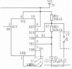
The generation of the second pulse is performed by a multi-resonant circuit composed of 555 timers. The circuit diagram is shown in Figure 2. When the switch is off, the 555 timer generates a pulse with a period of 1 second; when the switch is closed, the circuit has no signal output, so there is no pulse input in the 74LS192 counter, and the 74LS192 counter is maintained in the hold state, that is, the pause function is realized.

Figure 2 signal generation circuit
2.2 counting circuit
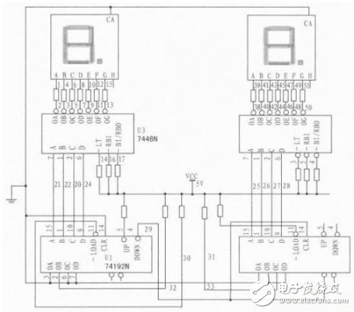
Using two 74LS192 counters as the one-bit (lower) and ten-bit (higher) countdown counters, the design only needs to count from "24" to "00", because the preset number is not "00", so choose The number of terminals (LOAD) to make the preset number. The clock pulse is input to the DOWN terminal of the 74LS192 counter bit (lower bit) through two AND gates respectively. When the stop signal is transmitted from the stop control circuit, the clock pulse is interrupted, thereby implementing the circuit stop function. Among them, the lower borrowing output signal is used as a high-order clock pulse.
Two 741S192 counters are specifically connected:
Vcc, UP connected to +5V power supply, GND grounded;
After the clock pulse is output from the AND gate, it is connected to the low DOWN, and then from the lower BO' to the high DOWN;
Input low bit C, high bit B is connected to the power supply, other pins and CLR are grounded; LOAD is connected to the active end of switch C, and the other two pins of C are respectively connected to the active end of G and ground. The other two pins of G are connected to the power supply and ground respectively. The circuit is shown in Figure 3.

Figure 3 counting circuit
2.3 stop control circuit
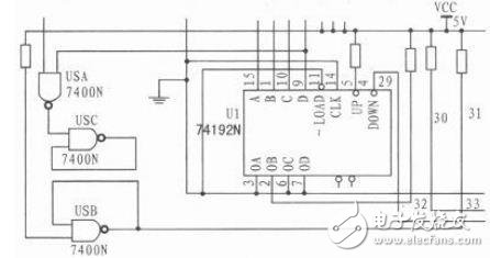
When the counter counts down to "0", the circuit needs to be forced to "24" and paused. Now select the counter to zero state for 24 seconds to "00", from each pin to the second NAND gate, when the counter transitions from the "00" state to "99", the state is converted to low with the NAND gate. The level (the rest of the time is high) controls the LD, causing the circuit to switch to "24". Since the number "99" is displayed for a short time, the "99" state is not seen in the transition from "00" to "24". The output of the flip-flop outputs a low level, leaving the 74LS192 in a hold state. This implements a control circuit that switches and stops. The circuit is shown in Figure 4.

Figure 4 stop control circuit
3.96Mm Terminal Block,Terminal Block Connector Right Angle,Right Angle F/M Pluggable Terminal Block,3.81Mm Pitch Plug-In Male Terminal Block
Dongguan City Yuanyue Electronics Co.Ltd , https://www.yuanyueconnector.com