Spec:
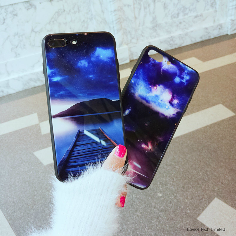
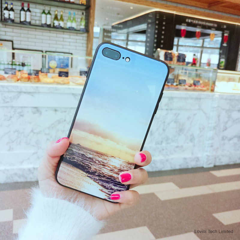
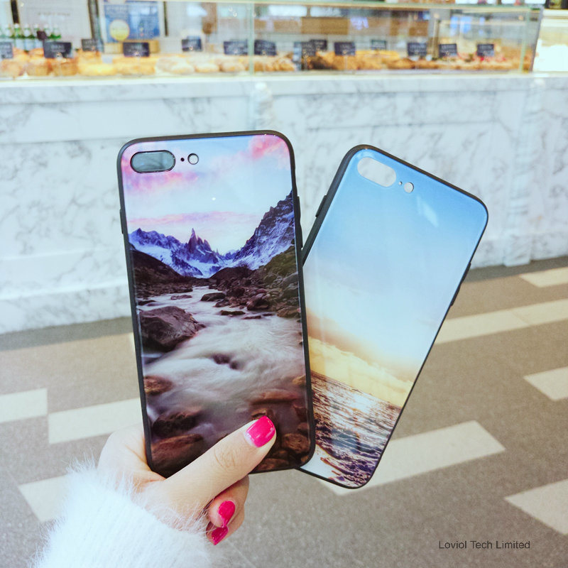
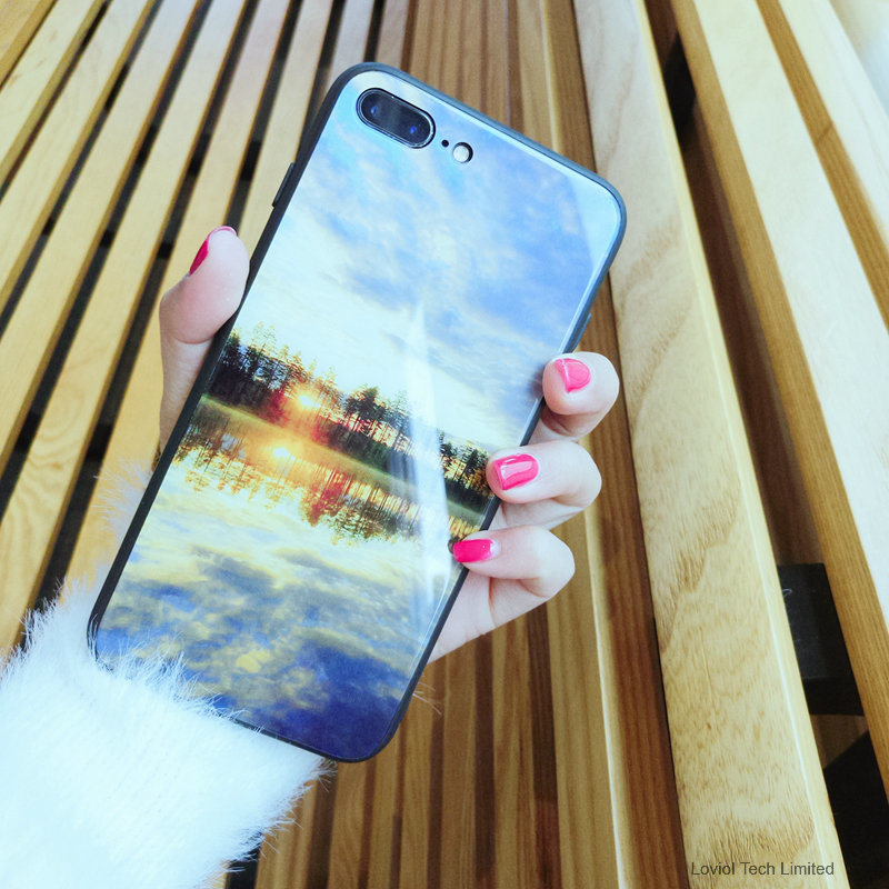
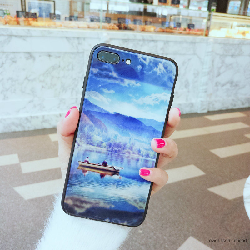
Protect camera design
360 degree full protection
Anti slip,anti shock, scratch proof
Flexible press keys,easy to operate
TPU side,eash to put on and take off
Popular design,smooth surface
More molds below,please feel free to enquire.
Â
| Loviol Tech Limited | |
| Glassy case molds | |
| Samsung | iPhone |
| S9 | iphone 5 |
| S9 Plus | iphone 6/6s |
| S8 | iphone 6 Plus |
| S8 Plus | iphone 7 |
| OPPO | iphone 8 |
| R15 | iphone 7 plus |
| R11s | iphone 8 plus |
| R11s Plus | iphone X |
| Vivo | Huawei |
| Vivo X21 | Huawei P20 |
| Vivo X20 | P20 Pro |
| Vivo X20 Plus | P10 |
| Â | P10 Plus |
| Â | Honor V10 |

Â
HDI PCB – High Density Interconnect PCB
High Density Interconnects (HDI) are used to meet the market demand for complex designs in smaller form factors across the majority of market segments, (Wireless, Telecom, Military, Medical, Semiconductor, and Instrumentation).
HDI Circuit boards, one of the fastest growing technologies in PCBs, HDI Boards contain blind and/or buried vias and often contain microvias of .006 or less in diameter.
They have finer lines and spaces always = <3mil They have a higher circuitry density than traditional circuit boards.
Andwin maintains years of experience with HDI products and was a pioneer of second generation microvias. now offer an entire family of microvia technology solutions for your next generation products.
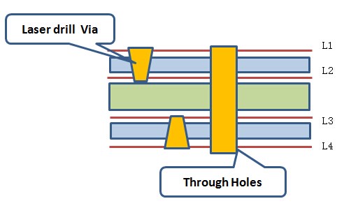
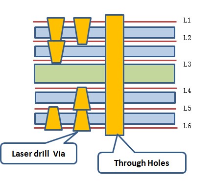
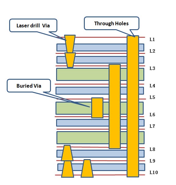
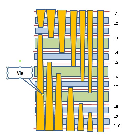
Stack up of HDI PCB
Stack up of 1 Step HDI PCB
Stack up of 2 step HDI PCB
Stack up of 2 steps HDI with blind via and buried via
HDI PCB Capabilities
|
Item |
Capabilities |
|
Layers |
3 - 16 Layers |
|
HDI Step |
3+N+3 |
|
Min.Line Width |
0.05mm (2 mil) |
|
Min.Line Space |
0.05mm (2 mil) |
|
Min.Annular ring |
0.1mm (4 mil) |
|
Min. Via |
0.1mm (4 mil) |
|
Max.Size |
500mm X 800mm |
|
Material |
FR4,High Tg220 |
|
Material thickness |
Start at 25um Plus copper |
|
Copper thickness |
0.3 OZ to 10 OZ (10um - 350um) |
About Us:
BentePCB is a professional PCB manufacturing which is focus on double side, multilayer, HDI PCB, rigid PCB and Flexible PCB mass production. The company was established on 2011.
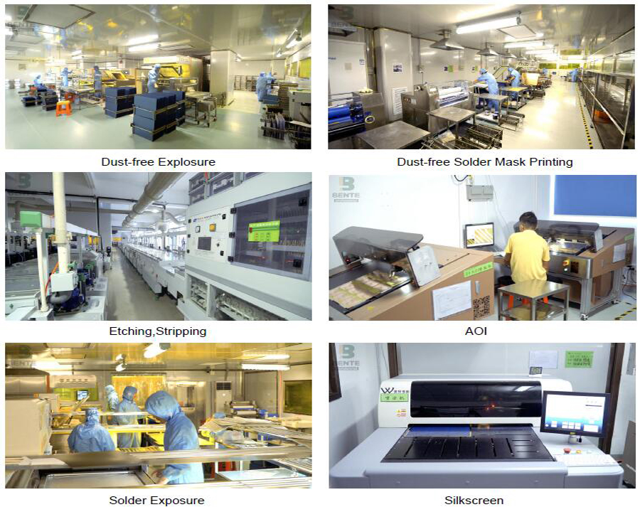
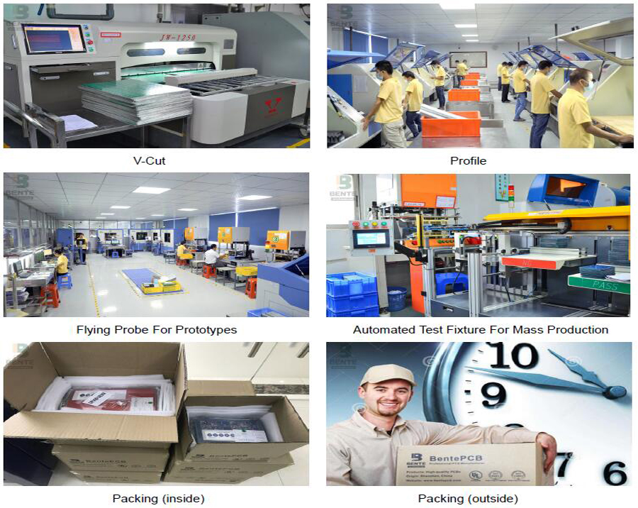
We have two factories together, The factory in Shenzhen is specialized in small and middle volume orders and the factory in Jiangxi is for big volumn.
Why Us?
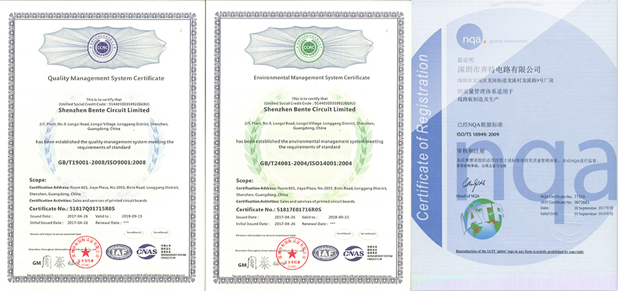
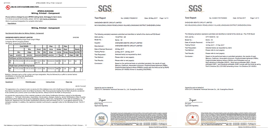
UL (E492586), ISO9001, ISO14001, TS16949, RoHS certified.
Turnover USD 10-50 million per year.
15,000 sqm area, 450 staff .
Mass Production from single to 16 layers.
Special Material:ROGERS, Arlon, Taconic.etc.
Client:Huawei, SAMSUNG, Malata, Midea,Texas Instruments.etc.
Certification(UL:E492586, TS16949, ISO14001, ISO9001,RoHS):
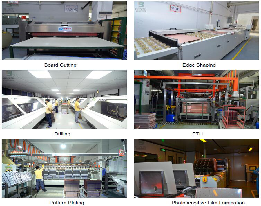
Factory Tour:
Exhibition:
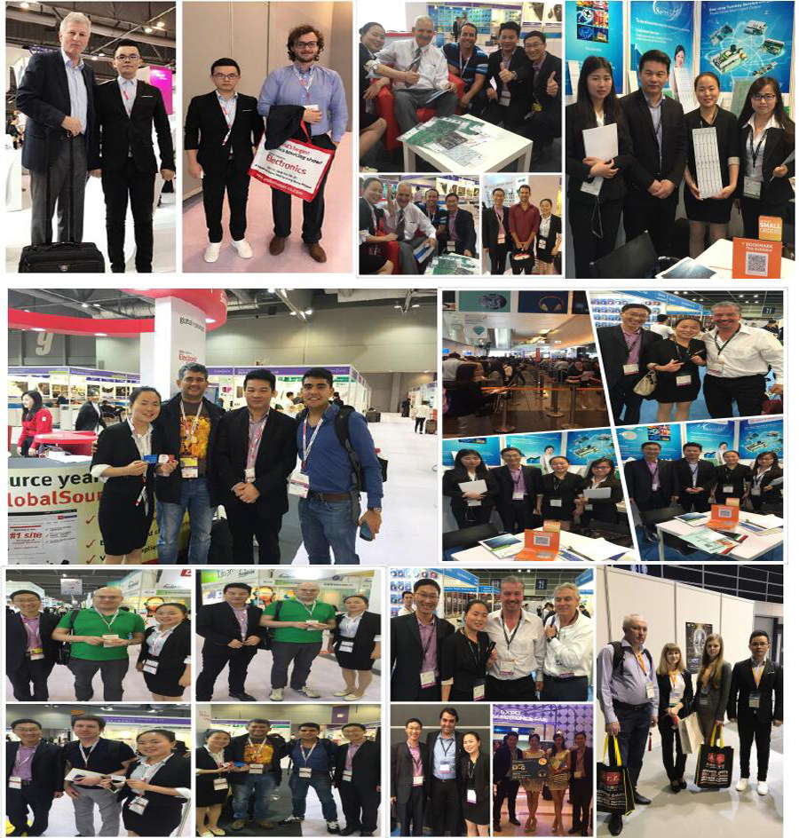
We Took part in the famous exhibitions over the past years,and got highly appreciation from the top experts,as well as cooperated tightly with them.
Delivery:
BentePCB offers flexible shipping methods for our customers, you may choose from one of the methods below.

FAQ:
Q1: What does BentePCB need for a customized PCB order?
A: The customers need to provide Gerber or pcb file.If you do not have the file in the correct format, you can send all the details related to the products.
Q2: What is your quotation policy?
A: For the PCB order in large quantity, BentePCB will send you the quotation based on the MOQ of the products concerned, and the price will be reasonable with good quality.
Q3: How long will you send us quotation ?
A: After all files were sent, 2 to 8 hours as per your file.
Q4:What is your minimum order quantity?
A:Our MOQ is 1 PCS.
Q5: How about the service BentePCB offered to the customers?
A: If you have any questions about our products or company, do not hesitate to send us your inquiry toour customer service representatives, Your satisfaction is our pursuits.
We don`t just sell PCBs .We sell sleep.

HDI PCB
HDI PCB, HDI Prototype PCB ,HDI Circuit Board, HDI PCB Boards
Shenzhen Bente Circuit Limited , http://www.bentegroup.com