Designing high-speed systems requires more than just high-speed components, but also a genius and careful design. The importance of device simulation is the same as the digital aspect. In high-speed systems, the noise problem is a fundamental consideration. High frequencies generate radiation and cause interference. The speed of the edge extremes can produce ringing, reflection, and crosstalk. If not suppressed, these noises can seriously impair the performance of the system.   
First, to achieve efficient design and efficient design of PCB automatic wiringAlthough the current EDA tools are very powerful, as PCB size requirements become smaller and the device density becomes higher and higher, PCB design is not difficult. How to achieve high PCB throughput and shorten design time? This article describes the design tips and key points of PCB planning, layout, and routing. PCB design time is getting shorter and shorter, smaller and smaller board space, higher device density, extremely harsh layout rules and large size components make the designer's work more difficult. In order to solve the design difficulties and speed up the market launch, many manufacturers now prefer to use dedicated EDA tools to achieve PCB design. However, dedicated EDA tools do not produce the desired results, nor can they achieve 100% throughput, and they are messy, and usually take a lot of time to complete the rest of the work.
There are a lot of EDA tools available on the market, but they are similar except for the terms and function keys used. How to use these tools to better realize the PCB design? Careful analysis of the design and careful setup of the tool software before starting the wiring will make the design more compliant. Below are the general design procedures and procedures.
1, determine the number of layers of the PCB
Board size and number of wiring layers need to be determined early in the design process. If the design requires the use of high-density ball grid array (BGA) components, the minimum number of routing layers required for wiring these devices must be considered. The number of wiring layers and the stack-up method directly affect the wiring and impedance of the printed wiring. The size of the board helps determine the stacking and line width to achieve the desired design.
For many years, people have always thought that the lower the number of board layers, the lower the cost, but there are many other factors that affect the manufacturing cost of the board. In recent years, the cost difference between multilayer boards has been greatly reduced. At the beginning of the design, it is better to use more circuit layers and evenly distribute the copper to avoid a small number of signals that do not meet the defined rules and space requirements at the end of the design, and thus be forced to add new layers. Careful planning before design will reduce a lot of trouble in wiring.
2, design rules and restrictions
The autorouting tool itself does not know what to do. To complete the routing task, the routing tool needs to work under the correct rules and constraints. Different signal lines have different wiring requirements, and all special required signal lines are classified, and different design classifications are also different. Each signal class should have priority. The higher the priority, the stricter the rules. The rules relate to the width of the trace, the maximum number of vias, the parallelism, the interaction between the signal lines, and the limitations of the layers, which have a large impact on the performance of the routing tool. Careful consideration of design requirements is an important step in successful cabling.
3, the layout of the components
To optimize the assembly process, the Manufacturability Design (DFM) rules place restrictions on the component layout. If the assembly department allows the components to move, the circuit can be properly optimized for easier automatic routing. The defined rules and constraints affect the layout design.
The layout path (rouTIng channel) and via area should be considered in the layout. These paths and areas are obvious to the designer, but the automatic routing tool only considers one signal at a time. By setting the wiring constraints and setting the layers of the signal lines, the routing tools can be imagined by the designer. That completes the wiring.
4, fanout design
In the fan-out design phase, for the auto-wiring tool to connect the component pins, each pin of the surface mount device should have at least one via so that the board can perform the inner layer when more connections are needed. Connectivity, online testing (ICT) and circuit reprocessing.
In order to maximize the efficiency of the automatic routing tool, it is important to use the largest via size and trace as much as possible, with an interval of 50 mils. Use a via type that maximizes the number of routing paths. When performing fan-out design, consider the online test of the circuit. Test fixtures can be expensive and are usually ordered when they are ready for full production. It is too late to consider adding nodes to achieve 100% testability.
After careful consideration and prediction, the design of the circuit online test can be carried out at the beginning of the design, implemented in the later stage of the production process, and the type of via fanout is determined according to the wiring path and the circuit online test. The power supply and grounding also affect the wiring and fanout design. . To reduce the inductive reactance of the filter capacitor connection, the via should be placed as close as possible to the surface mount device pins. If necessary, manual routing can be used, which may affect the originally proposed routing path and may even cause you to re- Consider which via is used, so you must consider the relationship between via and pin inductance and set the priority of the via specification.
5, manual wiring and key signal processing
Although this article focuses on the problem of automatic routing, manual routing is an important process for printed circuit board design now and in the future. Manual routing helps the automated routing tool complete the routing work. As shown in FIG. 2a and FIG. 2b, by manually routing and fixing the selected network (net), a path that can be relied upon for automatic routing can be formed.
Regardless of the number of critical signals, these signals can be routed first, manually wired, or combined with an automated routing tool. Critical signals must usually be carefully designed to achieve the desired performance. After the wiring is completed, the relevant engineering personnel will check these signal wirings, which is relatively easy. After the check is passed, the lines are fixed and the remaining signals are automatically routed.
6, automatic wiring
Wiring of critical signals requires consideration of controlling some electrical parameters during routing, such as reducing distributed inductance and EMC, and wiring for other signals. All EDA vendors offer a way to control these parameters. After understanding the input parameters of the automatic routing tool and the influence of the input parameters on the wiring, the quality of the automatic wiring can be guaranteed to a certain extent.
General rules should be used to automatically route signals. By setting constraints and disabling the routing area to define the layers used for a given signal and the number of vias used, the routing tool can be automatically routed according to the engineer's design philosophy. If there are no restrictions on the number of layers and the number of vias used in the automatic routing tool, each layer will be used for automatic routing and many vias will be created.
After setting the constraints and the rules created by the application, the automatic routing will achieve similar results as expected. Of course, some finishing work may be required, and other signals and network wiring space need to be ensured. After a part of the design is completed, fix it to prevent it from being affected by the rear wiring process.
The same steps are used to route the remaining signals. The number of wirings depends on the complexity of the circuit and the general rules you define. After each type of signal is completed, the constraints of the remaining network cabling are reduced. But what comes along is that many signal wiring requires manual intervention. Today's automated routing tools are very powerful and typically complete 100% wiring. However, when the automatic routing tool does not complete all signal routing, the remaining signals need to be manually routed.
7. Design points for automatic wiring include:
7.1 Change the settings slightly, try a variety of path wiring;
7.2 Keep the basic rules unchanged, try different wiring layers, different traces and spacing widths, and different line widths, different types of vias such as blind holes, buried holes, etc., to observe how these factors affect the design results;
7.3 Let the routing tools handle the default networks as needed;
The less important the 7.4 signal is, the more freedom the automatic routing tool will have to route it.
8, wiring finishing
If the EDA tool you are using can list the routing length of the signal, check the data and you may find that some signal routing with very few constraints is very long. This problem is easier to handle, and manual editing can reduce signal routing length and reduce the number of vias. In the finishing process, you need to determine which wiring is reasonable and which wiring is unreasonable. As with manual wiring design, the automatic routing design can also be organized and edited during the inspection process.
9, the appearance of the board
Previous designs often pay attention to the visual effects of the board, which is different now. The automatically designed circuit board is no more aesthetically pleasing than the manual design, but it meets the specified requirements in terms of electronic characteristics, and the complete performance of the design is guaranteed.
Two: High-speed PCB design to solve the nine rules of EMI problemsAs the signal rise time decreases and the signal frequency increases, the EMI problem of electronic products is more and more concerned by electronic engineers. Almost 60% of EMI problems can be solved by high-speed PCB. Here are the nine rules:
Rule 1: High-speed signal routing rules

In high-speed PCB design, critical high-speed signal lines such as clocks need to be shielded. If there is no shielding or only part of the shielding, it will cause EMI leakage. It is recommended to shield the wire, every 1000 mil, punch the ground.
Rule 2: Closed-loop rules for high-speed signals
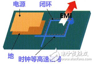
Due to the increasing density of PCB boards, many PCB LAYOUT engineers are prone to a mistake in the process of routing, that is, high-speed signal networks such as clock signals, which produce closed-loop results when multi-layer PCBs are routed. Such a closed loop result will produce a loop antenna that increases the radiant intensity of EMI.
Rule 3: Route-opening rules for high-speed signals
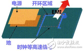
Rule 2 mentions that the closed loop of a high speed signal will cause EMI radiation, however open loop will also cause EMI radiation.
A high-speed signal network, such as a clock signal, produces a linear antenna that increases the radiant intensity of EMI once it has an open loop result in a multi-layer PCB trace.
Rule 4: Characteristic impedance continuous rules for high speed signals
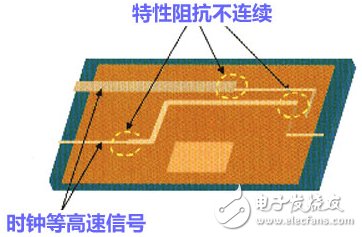
For high-speed signals, the continuity of the characteristic impedance must be ensured when switching between layers. Otherwise, EMI radiation will increase. That is to say, the width of the wiring of the same layer must be continuous, and the trace impedance of different layers must be continuous.
Rule 5: Wiring Direction Rules for High Speed ​​PCB Design
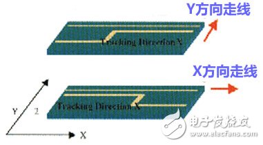
The traces between adjacent two layers must follow the principle of vertical traces, otherwise crosstalk between lines will be caused, and EMI radiation will be increased.
In short, the adjacent wiring layers follow the horizontal and vertical wiring directions, and the vertical wiring can suppress crosstalk between lines.
Rule 6: Topological rules in high-speed PCB design
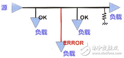
In high-speed PCB design, the control of the characteristic impedance of the circuit board and the design of the topology under multi-load conditions directly determine the success or failure of the product.
The illustration shows a daisy chain topology, which is generally used in the case of several Mhz. A star-shaped symmetrical structure at the back end is recommended for high-speed PCB design.
Rule 7: Resonance rules for the length of the trace
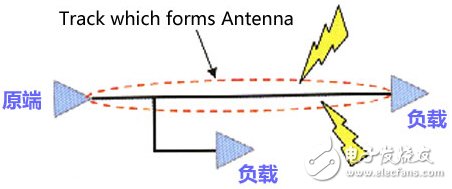
Check that the length of the signal line and the frequency of the signal constitute resonance, that is, when the wiring length is an integral multiple of the signal wavelength 1/4, the wiring will resonate, and the resonance will radiate electromagnetic waves, causing interference.
Rule eight: Return path rules
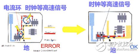
All high speed signals must have a good return path. As much as possible, ensure that the return path of high-speed signals such as clocks is minimized. Otherwise, the radiation is greatly increased, and the magnitude of the radiation is proportional to the area surrounded by the signal path and the return path.
Rule 9: Decoupling Capacitor Placement Rules for Devices
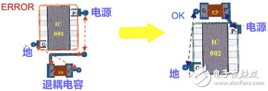
The placement of the decoupling capacitors is very important. Unreasonable placement does not result in decoupling. The principle is: close to the pin of the power supply, and the area enclosed by the power supply trace and ground of the capacitor is the smallest.
Third, high-speed PCB design rules summary and cause analysis1. If the PCB clock frequency exceeds 5MHZ or the signal rise time is less than 5ns, it is generally necessary to use a multi-layer board design.
Reason: The signal loop area of ​​the multi-layer board design can be well controlled.
2. For multi-layer boards, the key wiring layers (clock lines, buses, interface signal lines, RF lines, reset signal lines, chip select signal lines, and
The layers of various control signal lines and the like should be adjacent to the complete ground plane, preferably between the two ground planes.
Reason: The key signal lines are generally strong radiation or extremely sensitive signal lines. The wiring near the ground plane can reduce the signal loop area.
Reduce its radiation intensity or improve its anti-interference ability.
3. For single-layer boards, both sides of the key signal lines should be packaged.
Reason: The key signal is wrapped on both sides. On the one hand, the signal loop area can be reduced, and crosstalk between the signal line and other signal lines can be prevented.
4. For the double-layer board, the projection plane of the key signal line has a large area of ​​paving, or the same as the single panel.
Cause: The key signal of the multi-layer board is the same as the ground plane.
5. In a multi-layer board, the power plane should be retracted by 5H-20H (H is the distance between the power source and the ground plane) relative to its adjacent ground plane.
Cause: The power plane is retracted relative to its return ground plane to effectively suppress edge radiation problems.
6. The projection plane of the wiring layer should be in the area of ​​its reflow plane layer.
Cause: If the wiring layer is not in the projected area of ​​the reflow plane layer, it will cause edge radiation problems and increase the signal loop area.
This results in an increase in differential mode radiation.
7. In the multi-layer board, the TOP and BOTTOM layers of the single board should have no signal lines larger than 50 MHz.
Reason: It is best to move the high frequency signal between two planar layers to suppress its radiation to the space.
8. For a board with a board-level operating frequency greater than 50MHz, if the second layer and the penultimate layer are wiring layers, the TOP and BOOTTOM layers
Ground copper foil should be laid.
Reason: It is best to move the high frequency signal between two planar layers to suppress its radiation to the space.
9. In a multi-layer board, the main working power plane of the board (the most widely used power plane) should be in close proximity to its ground plane.
Cause: The power plane and the ground plane are adjacent to each other to effectively reduce the power circuit loop area.
10. In a single-layer board, there must be a ground line near the power supply line and its parallel and parallel lines.
Cause: Reduce the power supply loop area.
11. In the double-layer board, there must be a ground line near the power supply line and its parallel and parallel lines.
Cause: Reduce the power supply loop area.
12. In the layered design, try to avoid the adjacent layout of the wiring layer. If the wiring layers cannot be avoided, the two wiring layers should be properly extended.
The layer spacing between the layers reduces the layer spacing between the wiring layer and its signal loop.
Cause: Parallel signal traces on adjacent wiring layers can cause signal crosstalk.
13. Adjacent plane layers should avoid overlapping their projection planes.
Cause: When the projections overlap, the coupling capacitance between the layers causes the noise between the layers to couple with each other.
14, PCB layout design, should fully comply with the design principle of the straight line along the signal flow, try to avoid back and forth.
Cause: Avoid direct signal coupling and affect signal quality.
15. When multiple module circuits are placed on the same PCB, digital circuits and analog circuits, high-speed and low-speed circuits should be laid out separately.
Cause: Avoid mutual interference between digital circuits, analog circuits, high-speed circuits, and low-speed circuits.
16. When there are high, medium and low speed circuits on the circuit board, the high and medium speed circuits should be kept away from the interface.
Cause: Avoid high frequency circuit noise radiating outward through the interface.
17. Unit circuits or devices with large current changes (such as power supply modules: input and output terminals, fans and relays) should be placed nearby.
Energy storage and high frequency filter capacitors.
Cause: The presence of a storage capacitor can reduce the loop area of ​​the high current loop.
18. The filter circuit of the power input port of the circuit board should be placed close to the interface.
Cause: Avoid that the already filtered line is recoupled.
19. On the PCB, the filtering, protection, and isolation of the interface circuitry should be placed close to the interface.
Cause: The effects of protection, filtering, and isolation can be effectively achieved.
20. If there are both filtering and protection circuits at the interface, the principle of first filtering and filtering should be followed.
Reason: The protection circuit is used to perform external overvoltage and overcurrent suppression. If the protection circuit is placed behind the filter circuit, the filter circuit will be
Overvoltage and overcurrent damage.
21. When layout, ensure that the filter circuit (filter), isolation, and input and output lines of the protection circuit are not coupled to each other.
Cause: The input and output traces of the above circuit will weaken the filtering, isolation or protection effect when they are coupled to each other.
22. If the interface is “clean†on the board, the filtering and isolation devices should be placed in isolation between “clean†and the working ground.
Bring it.
Cause: Avoid filtering or isolating devices that are coupled to each other through plane layers, weakening the effect.
23. “Cleanâ€, no other components other than filtering and guarding devices.
Reason: The purpose of the "clean" design is to ensure that the interface radiation is minimal and that the "clean" is easily interfered by external interference, so "dry"
Do not have other unrelated circuits and devices on the net ground.
24, crystal, crystal, relay, switching power supply and other strong radiation devices away from the single-board interface connector at least 1000mil.
Cause: The interference will radiate directly or out of the outgoing cable to radiate outward.
25, sensitive circuits or devices (such as reset circuit, WATCHDOG circuit, etc.) away from the edge of the board, especially the side edge of the board interface to
Less 1000mil.
Cause: Similar to a single board interface, etc. is the most easily coupled by external interference (such as static electricity), like reset circuit, watchdog power
Sensitive circuits such as roads can easily cause system misoperation.
26. The filter capacitors for IC filtering should be placed as close as possible to the power supply pins of the chip.
Cause: The closer the capacitor is to the pin, the smaller the area of ​​the high-frequency circuit, and the smaller the radiation.
27. For the series matching resistor at the beginning, it should be placed close to its signal output.
Reason: The starting series matching resistor is designed to add the output impedance of the chip output to the impedance of the series resistor equal to the trace.
The characteristic impedance, the matching resistor is placed at the end, and the above equation cannot be satisfied.
28, PCB traces can not have right angle or sharp angle routing.
Cause: A right-angled trace causes the impedance to be discontinuous, causing the signal to emit, resulting in ringing or overshoot, creating strong EMI emissions.
29. Try to avoid layering of adjacent wiring layers as much as possible. When it is unavoidable, try to make the traces in the two wiring layers perpendicular or parallel to each other.
Degree is less than 1000 mil.
Cause: Reduce crosstalk between parallel traces.
30. If the board has an internal signal routing layer, key signal lines such as clocks are placed on the inner layer (prioritizing the preferred wiring layer).
Cause: The key signal can be shielded by laying it on the internal trace layer.
31. It is recommended to cover the grounding line on both sides of the clock line. The grounding line should be grounded every 3000 mils.
Reason: Ensure that the potentials at each point on the ground are equal.
32. Clock, bus, RF line and other key signal traces: Other parallel lines in the same layer should meet the 3W principle.
Cause: Avoid crosstalk between signals.
33. The surface mount fuse, magnetic bead, inductor, and tantalum capacitor used for the power supply with current ≥1A should be no less than two vias connected to the plane.
Floor.
Cause: Reduce the equivalent impedance of the via.
34. The differential signal lines should be in the same layer, equal length, and walking line. Keep the impedance one: no, there is no other trace between the differential lines.
Reason: Ensure that the common mode impedance of the differential pair is equal, and improve its anti-interference ability.
35. The critical signal traces must not be routed across the partition (including the reference plane gap caused by vias and pads).
Cause: Routing across the partition will result in an increase in the signal loop area.
36. When the signal line is split across its recirculation plane, it is recommended to use bridge capacitors in the vicinity of signal cross-segmentation.
The value is 1nF.
Reason: When the signal crosses the segmentation, it often leads to an increase in the loop area. The bridge grounding method is artificially set as the signal loop.
37. Do not have other unrelated signal traces under the filter (filter circuit) on the board.
Cause: The distributed capacitance will weaken the filtering effect of the filter.
38. The input and output signal lines of the filter (filter circuit) cannot be parallel to each other and cross-routed.
Cause: Avoid direct noise coupling before and after filtering.
39. The critical signal line is ≥3H from the reference plane edge (H is the height of the line from the reference plane).
Cause: Suppresses the edge radiation effect.
40. For the metal case grounding element, the copper should be grounded on the top layer of the projection area.
Cause: The external capacitance and the immunity are improved by the distributed capacitance between the metal case and the grounded copper.
41. In single-layer or double-layer boards, attention should be paid to the design of “minimum loop area†when wiring.
Cause: The smaller the loop area, the smaller the external radiation of the loop, and the stronger the anti-interference ability.
42. When changing the signal line (especially the key signal line), the via should be designed near the layered via.
Cause: The signal loop area can be reduced.
43. Clock line, bus, RF line, etc.: The strong radiation signal line is far away from the interface outgoing signal line.
Reason: Avoid interference on the strong radiation signal line coupled to the outgoing signal line and radiate outward.
44. Sensitive signal lines such as reset signal lines, chip select signal lines, system control signals, etc. are far away from the interface outgoing signal lines.
Cause: The outgoing signal line of the interface often brings in external interference. When it is coupled to the sensitive signal line, it will cause the system to malfunction.
45. In single-panel and dual-panel, the trace of the filter capacitor should be filtered by the filter capacitor before the device pin.
Cause: The power supply voltage is filtered first and then the IC is powered, and the noise that the IC feeds back to the power supply is also filtered out by the capacitor.
46. ​​In single-panel or dual-panel, if the power cable is very long, add a decoupling capacitor to the ground every 3000mil. The capacitance is 10uF.
+1000pF.
Cause: The high frequency noise on the power line is filtered out.
47. The grounding wire and power cable of the filter capacitor should be as thick and short as possible.
Reason: Equivalent series inductance will reduce the resonant frequency of the capacitor and weaken its high frequency filtering effect.
As a mobile multi-purpose platform, tablet computers also provide many possibilities for mobile teaching. The touch-based learning & entertainment teaching platform allows children to efficiently improve their academic performance in a relaxed and pleasant atmosphere. Such tablet computers generally integrate two learning sections of various courses and systematic learning functions. Generally, it includes multi-disciplinary high-quality teaching resources. The education tablet has the following main functions: it has the functions of touch screen input, text editing, picture editing, data storage, data management, wired and wireless Internet access that ordinary tablet computers have; Management functions, search methods support manual search, query by keyword, query by time; text and pictures can be scanned and converted into documents to save.
Education Tablet,learning tablet,leaning machine,New learning tablet
Jingjiang Gisen Technology Co.,Ltd , https://www.jsgisengroup.com