60v to 220v inverter circuit production (six inverter circuit design schematic diagram)
The inverter consists of three parts: inverter circuit, logic control circuit and filter circuit. It mainly includes input interface, voltage start circuit, MOS switch tube, PWM controller, DC conversion loop, feedback loop, LC oscillation and output loop, load. And so on. The control circuit controls the operation of the entire system. The inverter circuit performs the function of converting from direct current to alternating current. The filter circuit is used to filter out unwanted signals. The working process of the inverter is like this. The operation of the inverter circuit can be further refined as follows: first, the oscillating circuit converts the direct current into alternating current; secondly, the coil boosts the irregular alternating current into a square wave alternating current; finally, the rectification causes the alternating current to become a sinusoidal alternating current via the square wave .
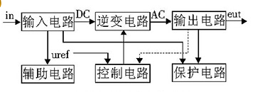
1. High conversion efficiency and fast startup;
2. Good safety performance: The product has five kinds of protection functions: short circuit, overload, over/under voltage and over temperature;
3, good physical properties: the product uses a full aluminum shell, good heat dissipation, surface hard oxidation treatment, good friction resistance, and can resist extrusion or impact of a certain external force;
4, with load adaptability and stability
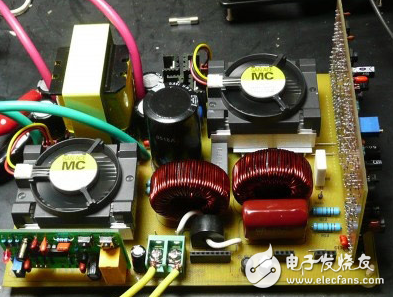
The transformer can be controlled by a 100W machine control transformer, the transformer core is taken apart, the secondary coil is removed, and the number of turns is recorded to calculate the number of turns per volt. Then rewind the secondary coil with a φ1.35mm enameled wire, first winding a 22V main coil, tapping in the middle, and then winding two 4V feedback coils with φ0.47 enameled wire. The layers of the coil are insulated with thick kraft paper. . After the coil is wound, the iron core is inserted, and the two 4V secondary wires are respectively connected with the main coil, and the end and the end are reversed. The voltage can be measured by the power. If the voltage increases after the connection between the 4V coil and the main coil, the connection is correct, and vice versa is wrong. You can change the connector.
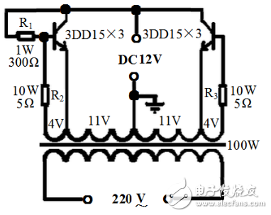
Two resistors R2 and R3 connected in series with the 4V coil can be made of resistance wire. The size of the resistor can be selected according to the output power. Generally, it is several ohms. When the output power is large, the resistance is smaller. The bias resistor uses 1W300Ω resistor. The resistor can also work, but it is better to pick one because the parameters of the tube are inconsistent and sometimes not vibrating. Triode selection: use three 3DD15 in parallel on each side, share six pipes. After the circuit is connected, check that there is no error, you can adjust the power, connect the battery, find a 100W incandescent lamp to load, turn on the switch, the bulb should be able to Normal illumination, if it can not normally emit light, can reduce the resistance of the base until it can normally emit light, then connect the color TV to see if it can start normally. It can also reduce the resistance of the base after normal startup. After the adjustment is completed, it can be used normally. It is.
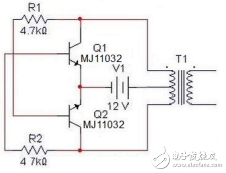
Inverter circuit (2)The inverter with only 4 components is simple to make and is good for general lighting. R1 and R2 are selected between 1.2k and 4.7k according to the difference between the triode and the transformer. The triode has no special requirements according to the capacity selection of the transformer. The large capacity uses the power point; the transformer can be used as a common control transformer, as long as there are two groups of 12V. . The 500W machine tool is used to control the transformer 0v-12V-24V, the Darlington tube MJ11032 for the triode, and the resistance is 4.7k. (The output is a square wave, not suitable for higher requirements).
Mainly composed of MOS field effect tube, common power transformer. Its output power depends on the power of the MOS FET and the power transformer, eliminating the cumbersome transformer winding, suitable for electronic enthusiasts in amateur production.
Circuit diagram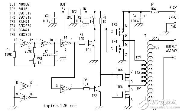
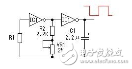
Here, a six-inverter CD4069 is used to form a square wave signal generator. In the circuit, R1 is a compensation resistor for improving the oscillation frequency instability caused by the change of the power supply voltage. The oscillation of the circuit is completed by charging and discharging the capacitor C1. The oscillation frequency is f=1/2.2RC. The maximum frequency of the circuit shown is: fmax=1/2.2&TImes;3.3&TImes;103&TImes;2.2&TImes;10-6=62.6Hz;minimum frequency fmin=1/2.2×4.3 ×103×2.2×10-6=48.0 Hz. Actual values ​​may vary slightly due to component errors. For other redundant inverters, the input is grounded to avoid affecting other circuits.
FET drive circuit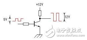
Since the maximum amplitude of the oscillating signal voltage output by the square wave signal generator is 0~5V, in order to fully drive the power switch circuit, the oscillating signal voltage is amplified to 0~12V by TR1 and TR2.
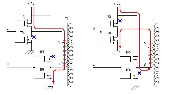
MOS FET power switch circuitThe following is a brief description of the working process of an application circuit composed of a C-MOS field effect transistor (enhanced MOS field effect transistor). The circuit combines an enhanced P-channel MOS FET with an enhanced N-channel MOS FET. When the input terminal is low level, the P-channel MOS FET is turned on, and the output terminal is connected to the positive terminal of the power supply. When the input terminal is at a high level, the N-channel MOS FET is turned on, and the output terminal is connected to the power ground.
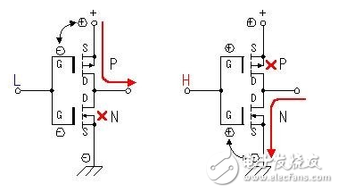
In this circuit, the P-channel MOS FET and the N-channel MOS FET are always operated in opposite states, and their phase input and output are opposite. Through this way we can get a larger current output. At the same time, due to the influence of leakage current, the gate voltage has not yet reached 0V, and when the gate voltage is less than 1 to 2V, the MOS field effect transistor is turned off. Different FETs have slightly different turn-off voltages. Because of this, the circuit does not cause a short circuit in the power supply because the two tubes are simultaneously turned on.
From the above analysis, we can draw the working process of the circuit part of the MOS FET in the schematic diagram.
This is a circuit diagram of household inverter power supply with excellent performance. The material is easy to take and the output power is 150W. The design frequency of this circuit is about 300Hz, the purpose is to reduce the volume and weight of the inverter transformer. Output waveform square wave. This inverter power supply can be used for home lighting in the event of power failure, fluorescent lamps for electronic ballasts, household appliances for switching power supplies, etc.
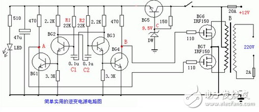
Capacitors C1 and C2 are made of polyester capacitors, triodes BG1-BG5 can be used with 9013:40V0.1A0.5W, and BG6-BG7 can be used with field effect transistors IRF150: 100V40A150W0.055 ohms. Do not connect the power tube first, measure the voltage of point A and point B to the ground, adjust R1 or R2 so that the voltages of the two points A and B are the same, so that the output square wave is symmetrical and the quiescent current is also the least.
Pay attention to the following items during installation: BG6 and BG7 must be soldered with a well-grounded soldering iron or cut off the power supply. The high current should be connected with a thick wire with a diameter of 2.5 mm or more, and the wiring should be as short as possible. The battery voltage is 12V and the capacity is 12AH or more. The power tube should be equipped with a suitable heat sink, for example, with a 100*100*3MM aluminum plate. If you want to increase the power, increase the power of the same type of power supply in parallel, and increase the power of the transformer accordingly.
Inverter circuit (5)The input end of the inverter is a car battery (+12V, 4.5Ah), and the output end is a power frequency square wave voltage (50Hz, 220V). The main circuit and control circuit block diagram of the system is shown in Figure 1. The typical two-stage transformation, DC/DC conversion and DC/AC inverter, is adopted. The 12V DC voltage is inverted into a high-frequency square wave by push-pull conversion, boosted by a high-frequency step-up transformer, and then rectified and filtered to obtain a stable DC voltage of about 320V; then, by bridge conversion, square wave inverter will be used. The stable DC voltage is inverted into a square wave voltage with an effective value slightly larger than 220V to drive the load. In order to ensure the reliable operation of the system, DC high-voltage side voltage signal, current signal and battery voltage signal are respectively collected and sent to SG3525A to realize voltage regulation, over-current protection and under-voltage by adjusting the duty cycle or shutdown pulse of the drive pulse. Protection and other functions.
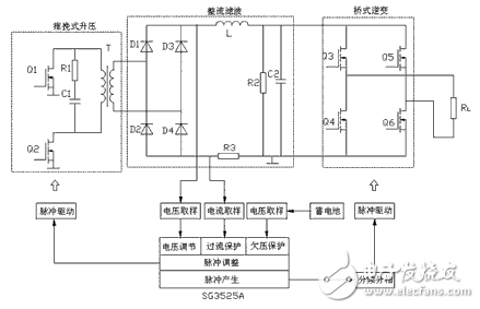
Diagram system main circuit and control circuit block diagram
Master chip SG3525A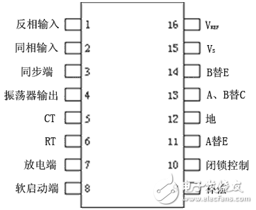
Determination of the oscillation frequency: The oscillation frequency is set by three external components RT, CT and RD, which are connected to the 6, 5, and 7 pins, respectively. The oscillation frequency is fOSC=1/CT(0.7RT+3RD), where 0.7RTCT is the timing capacitor charging time and 3RDCT is the timing capacitor discharging time. In order to make the frequency division and phase separation circuit obtain the 50Hz oscillation frequency, the design sets the oscillation frequency to 51.2kHz, taking CT=2000pF, RT=10kΩ, and RD=922Ω.
Output Pulse Width Adjustment: The PWM pulse width is controlled by the lower level of pins 9 and 8. The error amplifier U1 inside the chip amplifies the voltage feedback signal and the reference voltage signal and sends it to the inverting input terminal of the comparator U2. The input of the comparator positive input terminal is from the sawtooth wave on the capacitor CT, and the two are compared and output. Square wave pulse to control the duty cycle of the SG3525A internal output power amplifier tube. In this design, the 8-pin is grounded via a capacitor, and the 9-pin is connected to the feedback voltage of the DC/DC high-voltage DC voltage, thereby adjusting the stability of the output DC voltage.
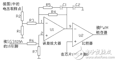
Figure Output DC High Voltage Regulation Schematic
In the figure, U1 is the error amplifier in SG3525A, 1, 2, and 9 are chip pins, respectively, and R1 to R7, C1, and C2 are external resistors and capacitors. The SG3525A's 16-pin output 5V reference voltage. Resistors R3, R4 and U1 form an inverse proportional operator, R4/R3 is its static amplification factor, and the larger the value, the higher the control accuracy. However, if the amplification is too large, it will cause oscillation. Therefore, the introduction of C1 and R5 makes the error amplifier an incomplete proportional integral controller. At this time, the static error amplification factor is constant, and the dynamic error amplification factor is reduced, which does not affect the control accuracy and avoids overshoot. Causes oscillation.
Frequency division and phase separation circuit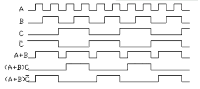
Windshield Cell Phone Mount,Car Windscreen Mobile Phone Holder,Car Windshield Cell Phone Holder,Car Windscreen Cell Phone Holder
Ningbo Luke Automotive Supplies Ltd. , https://www.car-phone-holder.com